HDL Workflow Advisor Tasks
HDL Workflow Advisor Tasks Overview
The HDL Workflow Advisor is a tool that supports a suite of tasks covering the stages of the FPGA design process. Some tasks perform model validation or checking. Other tasks run the HDL code generator or third-party tools. Each folder at the top level of the HDL Workflow Advisor contains a group of related tasks that you can select and run.
HDL Workflow Advisor is not available in Simulink® Online™.
For summary information on each HDL Workflow Advisor folder or task, select the folder or task icon, and then click the HDL Workflow Advisor Help button.
Set Target: The tasks in this category enable you to select the target device and map its I/O interface to the inputs and outputs of your model.
Prepare Model For HDL Code Generation: The tasks in this category check your model for HDL code generation compatibility. The tasks also report on model settings, blocks, or other conditions (such as algebraic loops) that impede code generation, and provide advice on how to fix such problems.
HDL Code Generation: This category supports all HDL-related options in the Configuration Parameters dialog box, including setting HDL code and test bench generation parameters, and generating code, test bench, or a cosimulation model.
FPGA Synthesis and Analysis: The tasks in this category support:
Synthesis and timing analysis through integration with third-party synthesis tools
Back annotation of the model with critical path and other information obtained during synthesis
FPGA-in-the-Loop Implementation: This category implements the phases of FIL, including providing block generation, synthesis, logical mapping, PAR (place-and-route), programming file generation, and a communications channel. These capabilities are designed for a particular board and tailored to your register transfer level (RTL) code. HDL Verifier™ is required for FIL.
Download to Target: The tasks in this category depend on the selected target device and potentially include:
Generation of a target-specific FPGA programming file
Programming the target device
Generation of a model that contains a Simulink Real-Time™ interface subsystem
ASIC Synthesis and Analysis: Use the tasks in this folder to:
Select a custom or default synthesis workflow for the Cadence® Genus synthesis tool.
Include custom setup, synthesis, and constraints files within the custom workflow.
Run synthesis through integration with third-party synthesis tools
See Also
Set Target Overview
In the Set Target folder, you can select a target FPGA device and define the interface generated for the device.
Set Target Device and Synthesis Tool: Select a target FPGA device and synthesis tools.
Set Target Reference Design: For
IP Core
                            Generation
workflow, select a reference design for your target device.Set Target Interface: For
IP Core
                            Generation
, andSimulink Real Time FPGA I/Oworkflows, use the target platform interface table to assign each port on your DUT to an I/O resource on the target device. Use Enable HDL DUT port generation for test points to create DUT output ports for the test point signals in the generated HDL code.Set Target Frequency: Select the target clock rate for the FPGA implementation of your design.
For more information on each Set Target task, select the task icon, and then click the HDL Workflow Advisor Help button.
See Also
Set Target Device and Synthesis Tool
The Set Target Device and Synthesis Tool task enables you to select an FPGA target device and an associated synthesis tool from a context menu that lists the devices that HDL Workflow Advisor supports.
Description
This task displays these options:
Target Workflow: A context menu that lists the possible workflows that HDL Workflow Advisor supports. Choose from:
Generic
                            ASIC/FPGA
FPGA-in-the-loop
Simulink Real-Time FPGA I/O
IP Core Generation
Target platform: A context menu that lists the devices the HDL Workflow Advisor supports. Not available for the Generic ASIC/FPGA workflow.
Synthesis tool: Select a synthesis tool, then select the Family, Device, Package, and Speed for your synthesis target.
If your synthesis tool is not one of the Synthesis tool options, see Synthesis Tool Path Setup. After you set up your synthesis tool path, click Refresh to make the tool available in the HDL Workflow Advisor.
Project folder: Specify the project folder name.
Tool version: This box displays the current synthesis tool version.
Allow unsupported version: When you are using an unsupported synthesis tool version, selecting this check box. You can continue to create a project with unsupported synthesis tool version. If you clear this check box, HDL Coder™ generates an error when you run this task. This option is unavailable when you are using the supported synthesis tool version.
It is not recommended to use the unsupported tool version because it can potentially cause synthesis failure. For more information on the list of supported tools, see HDL Language Support and Supported Third-Party Tools and Hardware
Note
If you select Microchip Libero SoC as the
Synthesis tool, you can
run only the Generic
ASIC/FPGA workflow. When you use these tools, the
Annotate Model with Synthesis Result task is not
available. In this case, you can run the workflow for synthesis, and then
view the timing reports to see the critical path.
Set Target Reference Design
The Set Target Reference Design task displays when IP Core Generation is selected as the Target Workflow and the Target Platform is not generic. This task displays the reference design input parameters and the tool version. A Reference design parameters section displays any custom parameters that you specify for the reference design.
Description
The task displays the following options:
Reference design: A context menu that lists the reference designs that HDL Coder supports and any custom reference designs that you specify. To learn more about creating a custom board and reference design, see Board and Reference Design Registration System.
Reference design tool version: A text box that displays the current reference design tool version. It is recommended to use a reference design tool version that is compatible with the supported tool version. If there is a tool version mismatch, HDL Coder generates an error when you run this task. The tool version mismatch can potentially cause the Create Project task to fail.
If you select the Ignore tool version mismatch check box, HDL Coder generates a warning instead of an error. You can attempt to continue with creating the reference design project.
Reference design parameters: A context menu that lists the parameters of the reference design. These parameters can be parameters available with the default reference designs that HDL Coder supports or parameters that you define for your custom reference design. For more information, see Define Custom Parameters and Callback Functions for Custom Reference Design.
FPGA Data Capture (HDL Verifier required): Generate and integrate the data capture IP into your reference design. Use FPGA data capture to observe signals from your design while the design is running on the FPGA. This feature captures a window of signal data from the FPGA and returns the data to MATLAB® or Simulink over an Ethernet, JTAG, or universal serial bus (USB) Ethernet connection.
Select the type of connection channel. If the target board and HDL Verifier support the connection, you can set this parameter to
JTAG,PL Ethernet,PS Ethernet, orUSB Ethernet. Then, map each signal that you want to capture to theFPGA Data Captureinterface in the Set Target Interface task.To use this capability, you must have the HDL Verifier hardware support packages installed and downloaded. See Download FPGA Board Support Package (HDL Verifier).
Key Considerations
FPGA data capture over a JTAG connection is available for Intel® and Xilinx® boards. FPGA data capture over an Ethernet or USB Ethernet connection is available for Xilinx boards only.
By default, the processing system (PS) Ethernet and USB Ethernet connections are available for these boards:
Zynq® UltraScale+™ MPSoC ZCU102 Evaluation Kit (with the
Default system with data capture with external DDR4 memory accessreference design)Zynq-7000 SoC ZC706 Evaluation Kit (with the
Data Capture IP with External DDR3 Memory Accessreference design)ZedBoard™ (with the
Default systemreference design)
To enable these connections for other boards, manually add the connection types in the
plugin_rdreference design definition file by using theaddFPGADataCaptureInterfacemethod before you start the HDL Workflow Advisor tool.By default, the programmable logic (PL) Ethernet connection is available for only the Artix®-7 35T Arty and Kintex®-7 KC705 boards. To enable this connection for other Xilinx boards that have the Ethernet physical layer (PHY), manually add the Ethernet media access controller (MAC) Hub IP in the
plugin_boardfile by using theaddEthernetMACInterfacemethod before you start the HDL Workflow Advisor tool.Adding the PL Ethernet connection in the
plugin_rdfile, without adding the Ethernet MAC Hub IP in theplugin_boardfile, results in an error.FPGA data capture in the HDL Workflow Advisor does not support SGMII interface.
Board IP Address: Specify the IP address of the Ethernet port on the target board as a dotted-quad value. The target IP address must be a set of four numbers consisting of integers in the range [0, 255] that are separated by three dots. The default value is
192.168.0.2.To enable this parameter, set FPGA Data Capture (HDL Verifier required) to
PL Ethernet.Insert AXI Manager (HDL Verifier required):
By default, HDL Coder adds the Insert AXI Manager (HDL Verifier required) parameter to all reference designs. When you set this parameter to
JTAG, the code generator inserts the JTAG AXI Manager IP into your reference design. When you set this parameter toPL Ethernet, the code generator inserts the UDP AXI Manager IP into your reference design.By using the AXI manager IP, you can easily access the AXI registers in the generated DUT IP core on a hardware board from MATLAB or Simulink through the JTAG or Ethernet connection. See also Set Up AXI Manager (HDL Verifier).
Key Considerations
By default, the PL Ethernet connection is available for only the Artix-7 35T Arty, Kintex-7 KC705, and Virtex®-7 VC707 boards. To enable this connection for other Xilinx boards that have the Ethernet physical layer (PHY), manually add the Ethernet MAC Hub IP in the
plugin_boardfile using theaddEthernetMACInterfacemethod before you start the HDL Workflow Advisor tool.
Set Target Interface
The Set Target Interface task displays properties of input and output ports on your DUT and enables you to map these ports to I/O resources on the target device.
Description
Set Target Interface displays the Target Platform Interface Table, which shows:
The name, port type (inputs and outputs), and data type for each port on your DUT.
A context menu listing the available I/O resources for the target device.
These resources are device-specific. For detailed information on each resource, see the documentation for your FPGA development board.
Set Target Interface
The Set Target Interface task that displays when Simulink Real-Time FPGA I/O or IP Core Generation is selected as the Target Workflow. Select a processor-FPGA synchronization mode and map your DUT input ports, output ports, and test points to I/O resources on the target device.
Description
Coprocessing mode is not supported for the Simulink Real-Time FPGA I/O workflow. For Processor/FPGA synchronization, select:
Free running if you do not want your processor and FPGA to be automatically synchronized.
Coprocessing – blocking if you want HDL Coder to generate synchronization logic for the FPGA automatically, so that the processor and FPGA run in tandem. Select this mode when FPGA execution time is short relative to the processor sample time and you want the FPGA to complete the synchronization before the processor continues.
This setting is saved with the model as the
ProcessorFPGASynchronization HDL block property for the
DUT block.
Selecting the Enable HDL DUT port generation for testpoints:
Marks test point signals for code generation. See Model and Debug Test Point Signals with HDL Coder.
Enables the Enable HDL DUT output port generation for test points configuration set option.
Refreshes the target interface table to display the test point output ports in the interface table.
The Target Platform Interface Table displays:
The name, port type (input, output, and test point), and data type for each port on your DUT.
A context menu listing the available I/O resources for the target device.
These resources are device-specific. For detailed information on each resource, see the documentation for your FPGA development board.
See Also
Set Target Frequency
Specify the target frequency for these workflows:
Generic ASIC/FPGA: Specify the target frequency that you want your design to achieve. HDL Coder generates a timing constraint file for that clock frequency and adds the constraint to the FPGA synthesis tool project that you create in the Create Project task. If the target frequency is not achievable, the synthesis tool generates an error.IP Core Generation: Specify the target frequency for HDL Coder to modify the clock module setting in the reference design to produce the clock signal with that frequency. Enter a target frequency value that is within the Frequency Range (MHz). If you do not specify the target frequency, HDL Coder uses the Default (MHz) target frequency.Simulink Real-Time FPGA I/O: For Speedgoat boards that are supported byXilinx ISE, specify the target frequency to generate the clock module to produce the clock signal with that frequency.The Speedgoat boards that are supported by
Xilinx Vivadouse theIP Core Generationworkflow infrastructure. Specify the target frequency for HDL Coder to modify the clock module setting in the reference design to produce the clock signal with that frequency. Enter a target frequency value that is within the Frequency Range (MHz). If you do not specify the target frequency, HDL Coder uses the Default (MHz) target frequency.
See Also
Prepare Model for HDL Code Generation Overview
The tasks in the Prepare Model For HDL Code Generation folder check the model for compatibility with HDL code generation. If a check encounters a condition that raises a code generation warning or error, the right pane of the HDL Workflow Advisor displays information about the condition and how to fix it. The Prepare Model For HDL Code Generation folder contains these checks:
Check Model Settings check expedites model checks by removing redundant checks. The check provides you the option to open the HDL Code Advisor checks in a separate window and run those checks.
Check FPGA-in-the-Loop Compatibility: Check model compatibility with FPGA-in-the-loop, specifically:
Not allowed: sink/source subsystems, single/double data types, zero sample time
Must be present: HDL Verifier
This option is available only if you select
FPGA-in-the-Loopfor Target workflow.Check USRP Compatibility: The model must have two input ports and two output ports of signed 16-bit signals.
This option is available only if you select
Customization for the USRP Devicefor Target workflow.
For summary information on each Prepare Model For HDL Code Generation task, select the task icon, and then click the HDL Workflow Advisor Help button.
See Also
Check Model Settings
Check Model Settings checks model-wide parameter settings for HDL code generation compatibility of the model.
Description
This check examines the model parameters for compatibility with HDL code generation and flags conditions that raise an error or a warning during code generation. The HDL Workflow Advisor displays a table with the following information about each condition detected:
Block: Hyperlink to the model configuration dialog box page that contains the error or warning condition.
Settings: Name of the model parameter that caused the error or warning condition.
Current: Current value of the setting.
Recommended: Recommended value of the setting.
Severity: Severity level of the warning or error condition. Minimally, fix settings that are tagged as
error.
This check provides a button to open the HDL Code Advisor checks in a separate window. Clicking Run This Task does not open the HDL Code Advisor checks. HDL Code Advisor can run additional HDL code generation compatibility checks not covered in this task. For more info, see HDL Coder Checks.
Tip
To set reported settings to their recommended values, click the Modify All button. You can then rerun the check again and proceed to the next check.
Check FPGA-in-the-Loop Compatibility
HDL Verifier checks model for compatibility with FPGA-in-the-loop processing.
See Also
Prepare DUT For FIL Interface Generation (HDL Verifier).
HDL Code Generation Overview
The tasks in the HDL Code Generation folder enable you to:
Set and validate HDL code and test bench generation parameters. Most parameters on the HDL Code Generation pane in the Configuration Parameters dialog box and the Model Explorer are supported.
Generate any or all of:
RTL code
RTL test bench
Cosimulation model
SystemVerilog DPI test bench
To run the tasks in the HDL Code Generation folder automatically, select the folder and click Run All.
Tip
After each task in this folder runs, HDL Coder updates the Configuration Parameters dialog box and the Model Explorer.
Set HDL Options
Optional task to open the HDL Coder Configuration Parameters dialog box.
Description
The Set HDL Options is an optional task. This task provides you with the option to open the HDL Coder Configuration Parameters dialog box in a separate window. Changes to the configuration parameters are used in the next HDL Coder Workflow Advisor task.
Note
Before doing this task, close the HDL Coder Configuration Parameters dialog box.
Limitations
When the Workflow Advisor window is open for the current design under test (DUT), these configuration parameters are disabled for editing:
Name of the DUT model or subsystem.
Name and path of the target code generation folder.
Name of the synthesis tool.
Device family selection.
Device selection.
Device package selection.
Device speed selection.
Target frequency.
If you make any changes to these configuration parameters, rerun all the previous Workflow Advisor tasks. If you change the name of the DUT model or subsystem, restart the Workflow Advisor and rerun all the Workflow Advisor tasks.
Generate RTL Code and Testbench
Select and initiate generation of RTL code, RTL test bench, cosimulation model, and RTL lint check report.
Description
The Generate RTL Code and Testbench task enables choosing what type of code or model that you want to generate. You can select any combination of the following:
Generate RTL code: Generate RTL code in the target language.
Generate test bench: Generate the test bench if HDL Test Bench is selected in HDL Coder Configuration Parameters > Test Bench > Test Bench Generation Output.
Generate validation model: Generate a validation model that highlights generated delays and other differences between your original model and the generated cosimulation model. With a validation model, you can observe the effects of streaming, resource sharing, and delay balancing.
The validation model contains the DUT from the original model and the DUT from the generated cosimulation model. Using the validation model, you can verify that the output of the optimized DUT is bit-true to the results produced by the original DUT.
Generate RTL lint check report: Generate an RTL lint check report for the generated HDL code by using the selected Lint tool. When you select this option, a new task Generate RTL Lint Check Report is enabled in the HDL Code Generation tasks folder.
Verify with HDL Cosimulation
Run this step to verify the generated HDL code using cosimulation between the HDL Simulator and the Simulink test bench. This step shows as a Workflow Advisor Task only if you:
Select Generate test bench in Generate RTL Code and Testbench.
Select Cosimulation model and specify a Simulation Tool in HDL Coder Configuration Parameters > Test Bench > Test Bench Generation Output.
Generate RTL Lint Check Report
Run this step to generate an RTL lint check report for the generated HDL code. This step appears as a Workflow Advisor Task only if you select Generate RTL lint check report in the Generate RTL Code and Testbench pane.
Description
This task displays these options:
Lint tool: Select a lint tool from the list. After you configure the lint tool path, click Refresh to display the available tool version in the HDL Workflow Advisor.
Tool version: View the current version of the selected lint tool.
Custom lint file: Specify the custom lint file name if you want to use a custom lint script. Leave this field empty to use the default lint script provided by the tool.
Skip this task: Select this option if you do not want the HDL Workflow Advisor to generate the RTL link check report.
For more information, see Generate RTL Lint Check Report Using HDL Workflow Advisor and Synopsys SpyGlass Lint Tool.
Generate RTL Code and IP Core
Select and initiate generation of RTL code and a custom IP core.
Description
In the Generate RTL Code and IP Core task, specify characteristics of the generated IP core:
IP core name: Enter the IP core name.
This setting is saved with the model as the
IPCoreNameHDL block property for the DUT block.IP core version: Enter the IP core version number. HDL Coder appends the version number to the IP core name to generate the output folder name.
This setting is saved with the model as the
IPCoreVersionHDL block property for the DUT block.IP core vendor name: Enter the IP core vendor name.
This setting is saved with the model as the
IPCoreVendorNameHDL block property for the DUT block.The vendor name must not start with a numeric character (for example,
23networkis invalid), and must not contain whitespace characters (for example,net workis invalid). The vendor name does not need to include a domain suffix such as.comor.net.Note
You can specify the vendor name only when you set the Target workflow to
IP Core Generationand the Synthesis tool toXilinx Vivado.IP core folder (not editable): HDL Coder generates the IP core files in the output folder shown, including the HTML documentation.
IP repository: If you have an IP repository folder, enter its path manually or by using the Browse button. The code generator copies the generated IP core into the IP repository folder.
Additional source files: If you are using a black box interface in your design to include existing Verilog®, SystemVerilog or VHDL® code, enter the file names. Enter each file name manually, separated with a semicolon (;) or by using the Add button.
This setting is saved with the model as the
IPCoreAdditionalFilesHDL block property for the DUT block.FPGA Data Capture storage type: Specify the memory type for storing captured data as one of these options:
Internal memory(default) — This memory type uses the internal BRAM resources of the FPGA to store captured data.External memory— This memory type uses external DDR, or any memory block connected to the data capture IP through an AXI4 interface, to store captured data.By default, the
External memoryoption is available for these boards:Zynq UltraScale+ MPSoC ZCU102 Evaluation Kit (with the
Default system with data capture
                                                  with external DDR4 memory access
reference design)Zynq-7000 SoC ZC706 Evaluation Kit (with the
Data Capture IP with External
                                                  DDR3 Memory Access
reference design)Kintex-7 KC705 Evaluation Kit (with the
External DDR3 Memory Access with Ethernet-Based FPGA Data Capturereference design)
To enable this option for other boards, configure the
plugin_rdreference design definition file by using theaddFPGADataCaptureInterfacemethod before you start the HDL Workflow Advisor tool.
Note
You can enable external memory only when targeting the Xilinx devices.
This setting is saved with the model as the
IPDataCaptureBufferTypeHDL block property for the DUT block.FPGA Data Capture buffer size: Specify the size of the memory in the generated IP core. The width of the memory is the total bit width of the data signals. By default, the buffer size is
128.This setting is saved with the model as the
IPDataCaptureBufferSizeHDL block property for the DUT block.Custom buffer size: Specify the size of the memory in the generated IP core, in powers of 2, 2N, where N is an integer from 7 to 31. By default, the buffer size is
128.Dependencies
To enable this parameter, set FPGA Data Capture buffer size to
custom.FPGA Data Capture maximum sequence depth: Specify the maximum sequence depth to capture data from an FPGA in one or more trigger stages. The maximum sequence depth is an integer that ranges from 1 to 10. By default, the maximum sequence depth is
1. To capture the specified data by providing a set of trigger conditions in multiple stages, set the maximum sequence depth to a value greater than 1.This setting is saved with the model as the
IPDataCaptureSequenceDepthHDL block property for the DUT block.Include capture condition logic in FPGA Data Capture: Select this parameter to include capture condition logic in the IP core. Include capture condition logic to use a capture condition to control which data to capture from the FPGA. The IP core evaluates the capture condition at each clock cycle and captures only the data that satisfies the capture condition. For more information on capture conditions, see Capture Conditions (HDL Verifier).
Set up a capture condition in the FPGA Data Capture (HDL Verifier) tool or the
hdlverifier.FPGADataReader(HDL Verifier) System object™.This setting is saved with the model as the
IncludeDataCaptureControlLogicEnableHDL block property for the DUT block.When you select Insert AXI Manager, AXI4 Subordinate ID Width value is adjusted for the DUT IP core that HDL Coder generates. When you select Insert AXI Manager and add custom IPs, you must specify the new adjusted subordinate ID width value. For example, when you select Insert AXI Manager and add custom IPs, if you get this error message during the Create Project task:
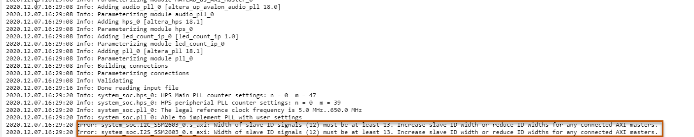
Regenerate the IP cores by setting the target platform as either Generic Intel or Generic Xilinx. Then map one of the DUT ports to the AXI4 interface, calculate the new width by using
New width = Base Width + log2(Number of AXI Masters +1), and enter the calculated width value in AXI4 Subordinate ID width. Add the regenerated IP cores with the new width values to the reference design folder. Right-click Create Project and select Run to Selected Task. In this example, the two custom IPs are I2C and I2s. The new calculated width is 13.Generate IP core report: Leave this option selected to generate HTML documentation for the IP core.
Enable readback on write registers: Select this option if you want to read back the value that is written to the AXI4 or AXI4-Lite registers by using the register interface. For more information, see Optimize Timing on Register Interface.
This setting is saved with the model as the
WriteRegisterReadbackHDL block property for the DUT block.Enable clock domain crossing on AXI4-Lite registers: Select this option if you want to run the register interface at a slower clock frequency than your high frequency design under test (DUT) algorithm. To use this option, set your Synthesis Tool to
Xilinx Vivado.This option can be used only for AXI4-Lite interfaces.Generate default register interface: Leave this option selected if you want to generate an HDL IP core with the register interface for signals such as clock, reset, ready, timestamp, and so on. If you want to generate a generic HDL IP core without any register interfaces, clear this check box. Make sure that you do not map any of the DUT ports to AXI4 or AXI4-Lite interfaces. You can map the ports to only External or Internal IO interfaces or to AXI4-Stream interface with TLAST mapping.
This setting is saved with the model as the
GenerateDefaultRegisterInterfaceHDL block property for the DUT block.Expose DUT clock enable input port: Select this option if you want to expose the DUT clock enable input port. Trigger the DUT from upstream IPs by using the clock enable input port. If your design has ports mapped to the register interface, this option is disabled.
Expose DUT clock enable output port: Select this option if you want to expose the clock enable output port to downstream IPs. Drive or synchronize downstream custom IPs by using the clock enable output port.
Register interface read pipeline: Specify the number of pipeline stages to insert in the read address decoder path by using the Register interface read pipeline setting in the Generate RTL Code and IP Core task of the IP Core Generation workflow. To learn more, see Optimize Timing on Register Interface.
Values:
0(default) | positive integerUse this parameter when you run into timing issues and the critical path is in the read address decoder. If you generate IP core for a model created before R2024b, and you have a value set for AXI4 Slave port to pipeline register ratio, HDL Coder sets Register interface read pipeline to
0.Offload large delays to external memory using: Specify whether to use a shared AXI4 Master interface or multiple individual AXI4 Master interfaces to offload large delays to external memory. You can set Offload large delays to external memory using to :
Shared Interface— A single AXI4 Master interface is exposed at the IP core boundary. HDL Coder generates an internal arbiter to manage access to external memory. Because only one AXI4 Master connection is required in the reference design, using this option simplifies integration.Independent interfaces— A separate AXI4 Master interface is generated for each delay. Arbitration is handled externally in the reference design, which allows the arbitration logic to run at a higher clock frequency. This option is better suited for real-time applications, but requires you to handle the arbitration outside or your IP core.
See Also
FPGA Synthesis and Analysis Overview
Create projects for supported FPGA synthesis tools, perform FPGA synthesis, mapping, and place/route tasks, and annotate critical paths in the original model.
Description
The tasks in the FPGA Synthesis and Analysis folder enable you to:
Create FPGA synthesis projects for supported FPGA synthesis tools.
Start supported FPGA synthesis tools, using the project files to perform synthesis, mapping, and place/route tasks.
Annotate your original model with critical path information obtained from the synthesis tools.
For a list of supported third-party synthesis tools, see Third-Party Synthesis Tools and Version Support.
The tasks in the folder are:
Create Project
Perform Synthesis and P/R
Annotate Model with Synthesis Result
See Also
Create Project
Create an FPGA synthesis project for a supported FPGA synthesis tool.
Description
This task creates a synthesis project for the selected synthesis tool and loads the project with the HDL code generated for your model.
When the project creation is complete, the HDL Workflow Advisor displays a link to the project in the right pane. Click this link to view the project in the synthesis tool project window.
- Synthesis objective
Select a synthesis objective to generate tool-specific optimization Tcl commands for your project. If you specify
None, no Tcl commands are generated.- Additional source files
Enter additional HDL source files that you want included in your synthesis project. Enter each file name manually, separated with a semicolon (;) or by using the Add Source button.
For example, you can include HDL source files (
.vhdor.v) or a constraint file (.ucfor.sdc).- Additional project creation Tcl files
Enter additional project creation Tcl files that you want to include in your synthesis project. Enter each file name manually, separated with a semicolon (;) or by using the Add Tcl button.
For example, you can include a Tcl script (
.tcl) to execute after creating the project.
See Also
Perform Synthesis and P/R Overview
Start supported FPGA synthesis tools to perform synthesis, mapping, and place/route tasks.
Description
The tasks in the Perform Synthesis and P/R folder enable you to start supported FPGA synthesis tool and:
Synthesize the generated HDL code.
Perform mapping and timing analysis.
Perform place and route functions.
For a list of supported third-party synthesis tools, see Third-Party Synthesis Tools and Version Support.
See Also
Perform Logic Synthesis
Start supported FPGA synthesis tool and synthesize the generated HDL code.
Description
The Perform Logic Synthesis task:
Starts the synthesis tool in the background.
Opens the previously generated synthesis project, compiles HDL code, synthesizes the design, and emits netlists and related files.
Displays a synthesis log in the Result subpane.
See Also
Perform Mapping
Starts supported FPGA synthesis tool and maps the synthesized logic design to the target FPGA.
Description
The Perform Mapping task:
Starts the synthesis tool in the background.
Runs a mapping process that maps the synthesized logic design to the target FPGA.
Emits a circuit description file for use in the place and route phase.
Emits pre-routing timing information for use in critical path analysis and back annotation of your source model.
Displays a log in the Result subpane.
Enable Skip pre-route timing analysis if your tool does not support early timing estimation. When this option is enabled, the Annotate Model with Synthesis Result task sets Critical path source to post-route.
See Also
Perform Place and Route
Starts the synthesis tool in the background and runs a Place and Route process.
Description
The Perform Place and Route task:
Starts the synthesis tool in the background.
Runs a Place and Route process that takes the circuit description produced by the previous mapping process, and emits a circuit description suitable for programming an FPGA.
Starts post-routing timing information for use in critical path analysis and back annotation of your source model.
Displays a log in the Result subpane.
If you select Skip this task, the HDL Workflow Advisor
executes the workflow, but omits the Perform Place and
Route task, marking it Passed. If you prefer
to do place and route work manually, you might want to select Skip
this task.
If Perform Place and Route fails, but you want to use the post-mapping timing results to find critical paths in your model, you can select Ignore place and route errors and continue to the Annotate Model with Synthesis Result task.
See Also
Run Synthesis
Starts Xilinx Vivado® and executes the Vivado Synthesis step.
If you do not want to do early timing estimation, enable Skip pre-route timing analysis.
Run Implementation
Starts Xilinx Vivado and executes the Vivado Implementation step.
If you select Skip this task , the HDL Workflow Advisor
omits the Run Implementation task, marking it
Passed. If you prefer to do place and route work manually,
select Skip this task.
If Run Implementation fails, you can select Ignore place and route errors and continue to the Annotate Model with Synthesis Result task.
Check Timing Report
If there are timing failures during this task, the task does not fail. You must check the timing report for timing failures.
Annotate Model with Synthesis Result
Analyzes pre- or post-routing timing information and visually highlights critical paths in your model.
Description
The Annotate Model with Synthesis Result task helps you to identify critical paths in your model. Depending on your option selection, the task analyzes pre- or post-routing timing information produced by the Perform Synthesis and P/R task group and visually highlights one or more critical paths in your model.
Note
If you select Cadence Genus or
Microchip Libero SoC as the
Synthesis tool, the Annotate Model with
Synthesis Result task is not available. Run the workflow to
synthesis, and then view the timing reports to see the critical path.
If you select Generate FPGA top level wrapper in the Generate RTL Code and Testbench task, Annotate Model with Synthesis Result is not available. To perform back-annotation analysis, clear the check box for Generate FPGA top level wrapper.
Input Parameters
- Critical path source
Select pre-route or post-route.
The pre-route option is unavailable when Skip pre-route timing analysis is enabled in the previous task group.
- Critical path number
You can annotate up to three critical paths. Select the number of paths that you want to annotate.
- Choose Model to Annotate
You can perform the annotation on the original as well as generated model. Select the
originalorgeneratedmodel that you want to annotate. For more information on generated model, see Generated Model and Validation Model.- Show all paths
Show critical paths, including duplicate paths.
- Show unique paths
Show only the first instance of a path that is duplicated.
- Show delay data
Annotate the cumulative timing delay on each path.
- Show ends only
Show the endpoints of each path, but omit the connecting signal lines.
Results and Recommended Actions
When the Annotate Model with Synthesis Result task runs to completion, HDL Coder displays the DUT with critical path information highlighted.
See Also
Download to Target Overview
The Download to Target folder supports the following tasks:
Generate Programming File: Generate an FPGA programming file.
Program Target Device: Download generated programming file to the target development board.
Generate Simulink Real-Time Interface (for Speedgoat target devices only): Generate a model that contains a Simulink Real-Time interface subsystem.
For summary information on each Download to Target task, select the task icon, and then click the HDL Workflow Advisor Help button.
See Also
Generate Programming File
The Generate Programming File task generates an FPGA programming file that is compatible with the selected target device.
Program Target Device
The Program Target Device task downloads the generated FPGA programming file to the selected target device.
Before executing the Program Target Device task, make sure that your host PC is properly connected to the target development board using the required programming cable.
Generate Simulink Real-Time Interface
The Generate Simulink Real-Time Interface task generates a model containing an interface subsystem that you can plug into a Simulink Real-Time model.
The naming convention for the generated model is:
gm_fpgamodelname_slrt
where fpgamodelname is the name of the original model.
FPGA-in-the-Loop (FIL) Implementation
Set FIL options and run FIL processing.
Set FPGA-in-the-Loop Options
Set the connection type, synchronization mode, option to generate the host interface script, board IP address, and board MAC address. Also, select additional files if required.
FPGA-in-the-Loop Connection
Select the FIL simulation connection method. The options in the drop-down menu
update depend on the connection methods supported for the target board you
selected. If the target board and HDL Verifier support the connection, you can choose
Ethernet, JTAG,
PCI Express, or USB
Ethernet.
MATLAB/FPGA Synchronization Mode
Select a mode for streaming data between MATLAB and the DUT. If the target board and FIL connection support, you can choose one of these modes:
Lockstep — In this mode, the DUT on the FPGA operates in lockstep with MATLAB. This mode is the default option and it is implicit in FIL simulation.
Free-running FPGA — In this mode, the DUT on the FPGA runs asynchronously with MATLAB. The hardware clock runs continuously inside the FPGA itself.
Note
For free-running FIL, the HDL Workflow Advisor:
Does not generate the Simulink verification model, as this mode works only when you use FIL with a MATLAB System object. It does not work when you use FIL with a Simulink block.
Always generates the host interface script.
For more information on these modes, see What Is Free-Running FPGA-in-the-Loop? (HDL Verifier).
Generate Host Interface Script
Select this option to generate a host interface script,
gs_,
where DUTName_interface_fil.mDUTNamefilObj object for interfacing with
the FPGA from MATLAB. The interface script contains MATLAB commands that connect to the hardware and program the FPGA, and
examples of how to exchange data with your algorithm as it runs on the
hardware.
Enable Data Buffering on FPGA
Select this option to enhance simulation performance. When selected, FIL utilizes BRAMs on the FPGA to buffer Ethernet packets in frame-based processing mode. Clear this parameter when BRAM resources are scarce in your design. Available for Ethernet connection only.
Board IP Address
Set the IP address of the board if it is not the default IP address (192.168.0.2).
Board MAC Address
Under most circumstances, you do not need to change the Board MAC address. If you connect more than one FPGA development board to a single computer (for which you must have a separate NIC for each board), you must change the Board MAC address. You must change the Board MAC address for additional boards so that each address is unique.
Additional Source Files
Select additional source files for the HDL design that is to be verified on the FPGA board, if required. HDL Workflow Advisor attempts to identify the file type. Change the file type in the File Type column if it is incorrect.
Set DUT I/O Ports
This step is enabled only when you select the free-running FPGA mode.
The HDL Workflow Advisor parses the input and output ports of your DUT from the top file. It infers each port type from the HDL port name. Verify and modify the port type as needed.
Build FPGA-in-the-Loop
During the build process:
FPGA-in-the-loop generates a FIL block named after the top-level module and places it in a new model.
After new model generation, FIL opens a Command Prompt. In this Command Prompt, the FPGA design software performs synthesis, fit, place-and-route, timing analysis, and FPGA programming file generation. When the process is complete, a message in the Command Prompt prompts you to close the window.
FPGA-in-the-loop builds a test bench model around the generated FIL block.
FPGA-in-the-loop generates a host interface script for interfacing with the FPGA from MATLAB if you select the Generate host interface script option in the Set FPGA-in-the-Loop Options task.
Embedded System Integration
Tasks in this folder integrate your generated HDL IP core into the embedded processor.
Create Project
Create project for embedded system tool.
In the message window, after the project is generated, you can click the project link to open the generated embedded system tool project.
- Embedded system tool
Embedded design tool.
- Project folder
Folder where your generated project files are saved.
- Synthesis objective
Select a synthesis objective to generate tool-specific optimization Tcl commands for your project. If you specify
None, no Tcl commands are generated.To learn how the synthesis objectives map to Tcl commands, see Synthesis Objective to Tcl Command Mapping.
- Enable IP caching
Create IP cache to reduce reference design synthesis time. When you enable IP caching, the code generator creates an IP cache. The
IP Core
                                Generation
workflow uses an out-of-context (OOC) workflow. This workflow synthesizes the IP in the reference design out of context from the top-level design. You can reuse this cache in subsequent project runs, which reduces reference design synthesis time. To learn more, see IP Caching for Faster Reference Design Synthesis.
Generate Software Interface
To generate the embedded C code, generate a Simulink software interface model with the IP core driver blocks. To verify the IP core functionality and connect to the onboard memory locations, generate a host interface model, host interface script, or both with the AXI Manager.
When you clear the Generate Simulink software interface model, Generate host interface model, and Generate host interface script check boxes, the HDL Workflow Advisor skips this task.
Description
In the Generate Software Interface task, specify a software interface that you want to generate for the IP core.
Generate Simulink software interface model — Select this parameter to generate a Simulink software interface model for an SoC device. The software interface model is your original model with the AXI driver blocks replacing the parts you want to run on hardware. This parameter is not available for standalone FPGA boards.
After you generate the Simulink software interface model, you can generate C code from it by using Embedded Coder®. If you do not have the Embedded Coder hardware support package for the target board installed, this parameter is not available. For example, if the target hardware board is a Zynq device, you must have the Embedded Coder Support Package for AMD SoC Devices installed.
Operating system — Select your target operating system.
Host target interface — Select an interface that communicates between your host machine and the target hardware. Use one of these options.
JTAG AXI Manager (HDL Verifier)— Use the JTAG interface to access AXI4 and AXI4-Lite registers on the target hardware. To enable this option, in the Set Target Reference Design task, set Insert AXI Manager (HDL Verifier required) toJTAGand in the Set Target Interface task, map each DUT signal that you want to capture to theAXI4orAXI4-Liteinterface.Ethernet AXI Manager (HDL Verifier)— Use the Ethernet interface to access AXI4 and AXI4-Lite registers on the target hardware. To enable this option, in the Set Target Reference Design task, set Insert AXI Manager (HDL Verifier required) toPL Ethernetand in the Set Target Interface task, map each DUT signal that you want to capture to theAXI4orAXI4-Liteinterface.Ethernet— Use the Ethernet interface to access the generated IP core deployed on your target hardware. This option is not available for standalone FPGA boards.
Generate host interface model — Select this parameter to generate a host interface model. The host interface model enables you to write to or read from the memory-mapped locations on the target hardware over a JTAG or Ethernet cable by using the AXI Manager Write and AXI Manager Read blocks.
To enable this parameter, set Host target interface to
JTAG AXI Manager (HDL Verifier)orEthernet AXI Manager (HDL Verifier).Generate host interface script — Select this parameter to generate a host interface script. The host interface script contains commands that enable you to connect to the target hardware and to write to or read from the generated IP core by using the AXI driver blocks or the AXI Manager.
Build FPGA Bitstream
Generate bitstream for embedded system.
- Run build process externally
Enable this option to run the build process in parallel with MATLAB. If this option is disabled, you cannot use MATLAB until the build is finished. This option is valid only when you use the
IP Core Generationworkflow.- Tcl file for synthesis build
To customize your synthesis build, save your custom Tcl commands in a file and select
Custom. Enter the file path manually or find the path by using the Browse button. The contents of your custom Tcl file are inserted between the Tcl commands that open and close the project.If you select
Customand want to generate a bitstream, the bitstream generation Tcl command must refer to the top file wrapper name and location either directly or implicitly. For example, the following Xilinx Vivado Tcl command generates a bitstream and implicitly refers to the top file name and location:launch_runs impl_1 -to_step write_bitstream
- Enable routed design checkpoint for build
Select this option to expedite bitstream generation time by using the design checkpoint from the previous build. This option is available only when using the Xilinx Vivado synthesis tool.
- Routed design checkpoint file for build
To use this option, select Enable routed design checkpoint for build. To use the default routed design checkpoint file, select
Default. The default file location ishdl_prj\checkpoint\system_routed.dcp. To use a custom routed design checkpoint file, selectCustomand provide the file path to your custom file location. This option is available only when using the Xilinx Vivado synthesis tool.- Routed design checkpoint file
To use this option, select
Customfor Routed design checkpoint file for build. Use this option to point to your custom routed design checkpoint file. After bitstream generation is completed the new routed checkpoint design file is written to the location specified in Routed design checkpoint file. This option is available only when using the Xilinx Vivado synthesis tool.- Maximum number of cores for build
Reduce bitstream generation times by using multiple logical cores of the PC. Use this option to choose the maximum number of PC cores to use. Selecting
synthesis tool defaultselects the maximum number of cores set in the synthesis tool. To manually select the maximum number of cores, select between2and32.
Program Target Device
Program the connected target SoC device. Specify the Programming method for the target device:
JTAG: Uses a JTAG cable to program the target SoC device.Download: This is the default Programming method. Copies the generated FPGA bitstream, device tree, and system initialization scripts to the SD card on the Zynq board and keeps the bitstream on the SD card persistently. To use this programming method, you do not need Embedded Coder. You can create an SSH object by specifying the IP Address, SSH Username, and SSH Password. HDL Coder uses the SSH object to copy the bitstream to the SD card and reprogram the board.
To define your own function to program the target device in your custom reference
design, you can use the Custom
Programming method. To use the custom programming, register the
function handle of the custom programming function by using the
CallbackCustomProgrammingMethod method of the
hdlcoder.ReferenceDesign class. For
example:
hRD.CallbackCustomProgrammingMethod = ...
    @parameter_callback.callback_CustomProgrammingMethod;
For more information, see Program Target FPGA Boards or SoC Devices.
ASIC Synthesis and Analysis Overview
In the ASIC synthesis and Analysis folder, you can create projects for supported ASIC synthesis tools, select either custom or default synthesis workflows, and perform ASIC synthesis tasks on the original model.
Description
The tasks within the ASIC Synthesis and Analysis folder enable you to:
Create ASIC synthesis projects using supported ASIC synthesis tools.
Use the project files to perform synthesis tasks on supported ASIC synthesis tools.
For a list of supported third-party synthesis tools, see Third-Party Synthesis Tools and Version Support.
The tasks in this folder are:
Create Project
Perform Synthesis and P/R
See Also
Create Project
Create an ASIC synthesis project for a supported ASIC synthesis tool.
Description
This task creates an ASIC synthesis project for the selected synthesis tool and loads the project with the HDL code generated for your model.
- Additional source files
Enter additional HDL source files (
.vhdor.v) that you want to include in your synthesis project. Enter each file name manually, separated with a semicolon (;), or use the Add Source button.- Synthesis workflow
Select a custom or default synthesis workflow.
If you select
customworkflow, you must add the Setup Tcl, Constraint Sdc, and Synthesis Tcl files.If you select
default, the tool automatically includes these files.
- Setup Tcl file
Enter the project creation Setup Tcl file that you want to include in your synthesis project. Enter each file name manually, separated with a semicolon (;) or use the Add Setup Tcl button.
- Constraint Sdc files
Enter the project creation Constraint Sdc files that you want to include in your synthesis project. Enter each file name manually, separated with a semicolon (;) or use the Add constraint Sdc button.
- Synthesis Tcl file
Enter the project creation Synthesis Tcl file that you want to include in your synthesis project. Enter each file name manually, separated with a semicolon (;) or use the Add synthesis Tcl button.
See Also
Perform Synthesis and P/R Overview
Start supported ASIC synthesis tools to perform synthesis.
Description
The tasks in the Perform Synthesis and P/R enable you to start a supported ASIC synthesis tool and synthesize the generated HDL code.
For a list of supported third-party synthesis tools, see Third-Party Synthesis Tools and Version Support.
See Also
Run Synthesis
Starts supported ASIC synthesis tool and synthesize the generated HDL code.
Description
The Run Synthesis task:
Opens the previously generated synthesis project, compiles the HDL code, synthesizes the design, and emits netlists and related files.
Starts the synthesis tool in the background unless you select the Run build process externally option.
Displays a synthesis log and provide links to the Parsed power report file and Parsed resource report file in the Result subpane.
- Run build process externally
Select this option to run the build process in an external console. If you do not select this option, you cannot use MATLAB until the build is finished.