Corporate Feed Divider Network for a Linear Patch Antenna Array
R2026bThis example shows how to integrate a corporate power divider with a microstrip patch antenna array to provide a signal feed to the antenna array. Corporate power dividers are used to divide, or combine, RF signals, either equally or unequally, from one port to multiple ports. The corporate power divider is available as a catalog element in RF PCB Toolbox™. The patch antenna array is built using the patchMicrostripInsetfed catalog element and pcbStack from Antenna Toolbox™.
Create Variables
Create common variables frequency f, and speed of light c.
f = 5e9;
c = physconst('lightspeed');
Create Corporate Power Divider
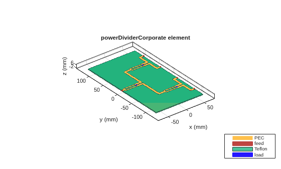
Use the powerDividerCorporate object to design a corporate power divider operating at 5 GHz. The default splitter element of the divider is an equal-divide Wilkinson splitter, used here. Other available splitter element settings are unequal-divide Wilkinson, and wide band Wilkinson. Port spacing is set to one wavelength at the operating frequency. In this example additional divider property values of splitter element substrate loss tangent, port line length, and ground plane width are specified. The default number of divider ports is four, used here. Other available port number settings are 2, 8, 16, and 32. Use the show function to visualize the divider.
pdc = powerDividerCorporate;
pdc = design(pdc,f);
pdc.SplitterElement.Substrate.LossTangent = 0;
pdc.PortSpacing = c/f;
pdc.PortLineLength = 10e-3;
pdc.GroundPlaneWidth = pdc.PortSpacing*4;
pdc;
figure,show(pdc);
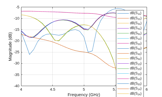
Use the sparameters function with Behavioral set to true.Plot s-parameters using the rfplot function. As the computation takes time, load the pre-computed mat file and plot the result using rfplot.
% out = sparameters(pdc,linspace(4e9,6e9,31),'Behavioral',true);
load pdc.mat
figure;
rfplot(sparPDC);
Create Inset Fed Patch Antenna
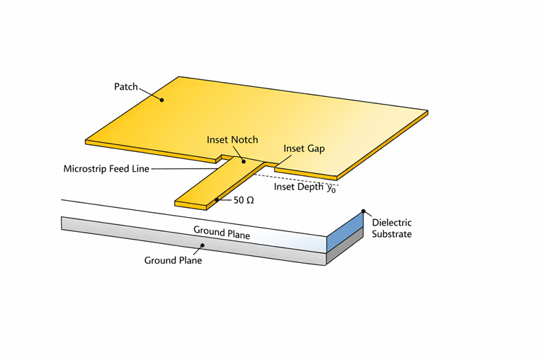
Use the patchMicrostripInsetfed object to design a microstrip inset fed patch with center operating frequency of around 5 GHz. In this type of design the feed line extends into patch cutouts, rather than connecting to the patch's edge, to provide impedance matching without need for additional matching components.
ant = patchMicrostripInsetfed;
ant.Substrate = dielectric('Teflon');
ant = design(ant,5e9)
ant =
patchMicrostripInsetfed with properties:
Length: 0.0207
Width: 0.0207
Height: 0.0010
Substrate: [1×1 dielectric]
PatchCenterOffset: [0 0]
FeedOffset: [-0.0207 0]
StripLineWidth: 0.0012
NotchLength: 0.0028
NotchWidth: 0.0021
GroundPlaneLength: 0.0414
GroundPlaneWidth: 0.0414
Conductor: [1×1 metal]
Tilt: 0
TiltAxis: [1 0 0]
Load: [1×1 lumpedElement]
ant.Height = 1.6e-3;
ant.Length = 20.5e-3;
ant.Width = 20.5e-3;
ant.StripLineWidth = pdc.PortLineWidth;
ant.NotchWidth = 7.1e-3;
ant.NotchLength = 5.9e-3;
Use the sparameters function to calculate the sparameters. As it takes more time to complete the simulation the pre-computed result is loaded.
% out = sparameters(ant,linspace(4e9,6e9,31)); Load the mat file and plot the sparameters using rfplot function.
load patch.mat
figure,rfplot(out);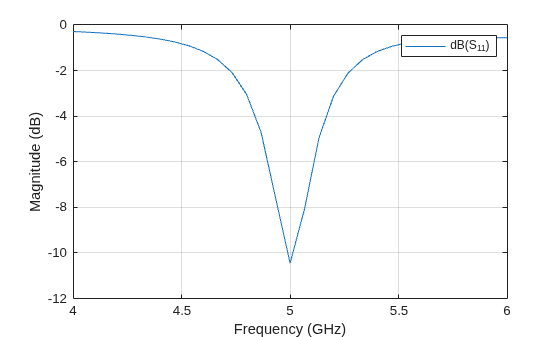
Create pcbStack for Antenna
Use the pcbStack object to convert the patch antenna into a pcb stack so that the shape of the top layer can be extracted from the Layers property. Convert into a linear array of 4 elements. The patch is extracted from the Layers property of the pcbStack and the shape is copied and converted into a linear array.
pcbant = pcbStack(ant);
TopLayer = pcbant.Layers{1};
TopLayer1 = copy(TopLayer);
for i = 2:4
    a = copy(TopLayer1);
    a = translate(a,[0,pdc.PortSpacing*(i-1),0]);
    TopLayer = TopLayer+a;
end
TopLayer = translate(TopLayer,[-ant.FeedLocation(1)+pdc.GroundPlaneLength/2,-pdc.PortSpacing*1.5,0]);
Create pcbComponent for Corporate Power Divider
Use the pcbComponent object and convert the corporate power divider into a PCB Component. Create a new pcbStack object to construct the cascade of power divider corporate and patch antennas. Assign all the properties of the pcbComponent to the pcbStack and then add the top layer of the corporate power divider with the patch antenna array and visualize it.
pcbcomp = pcbComponent(pdc);

pcbant1 = pcbStack;
pcbant1.BoardShape = pcbcomp.BoardShape;
pcbant1.BoardThickness =pcbcomp.BoardThickness;
pcbant1.Layers = pcbcomp.Layers;
pcbant1.FeedDiameter = pcbcomp.FeedDiameter;
pcbant1.FeedViaModel = pcbcomp.FeedViaModel;
pcbant1.FeedLocations = pcbcomp.FeedLocations;
pcbant1.Load = pcbcomp.Load;

a = pcbant1.Layers{1};
finalShape = a+TopLayer;
pcbant1.Layers{1} = finalShape;
feed = pcbant1.FeedLocations(1,:);
pcbant1.FeedLocations = feed;
gnd = pcbant1.Layers{3};
gnd.Length = gnd.Length+50e-3;
gnd.Width   = gnd.Width-20e-3;
gnd.Center(1) = 50e-3/2;
pcbant1.Layers{3} = gnd;
pcbant1.BoardShape = gnd;
figure,show(pcbant1);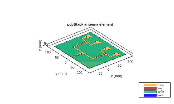
Use the mesh function to manually mesh the structure and use the sparameters function to compute the s-parameters. Generating a mesh and computing the result takes a lot of time as the structure is large compared to the wavelength. Hence the lines are commented out.
% figure,mesh(pcbant1,'MaxEdgeLength',6e-3);
% spar = sparameters(pcbant1,linspace(4e9,6e9,21));
% figure,pattern(pcbant1,4.9e9)
Load the precomputed result from PDCpatch.mat file and plot the results.
load PDCpatch.mat
figure;
rfplot(spar)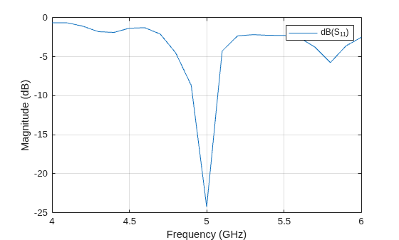
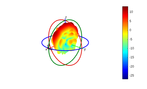
Use the patternCustom function to plot the 2-D or 3-D radiation pattern of an antenna magnitude, magE over the specified phi and theta angle vectors.
phi = az';
theta = (90-el);
MagE = pat';
figure;
patternCustom(MagE,theta,phi);