Clock and Data Recovery in SerDes System
High-speed analog SerDes systems use clock and data recovery (CDR) circuitry to extract
the proper time to correctly sample the incoming waveform. The CDR circuitry creates a clock
signal that is aligned to the phase and to some extent the frequency of the transmitted
signal. Phase tracking (first order CDR) is usually accomplished by using a nonlinear
bang-bang or Alexander phase detector that drives a voltage-controlled oscillator (VCO).
Frequency tracking (second order CDR) integrates any remaining phase errors and compensates
for gross differences between the transmitter reference clock and the receiver reference
clock. serdes.CDR and
serdes.DFECDR use
the first-order CDR algorithm.
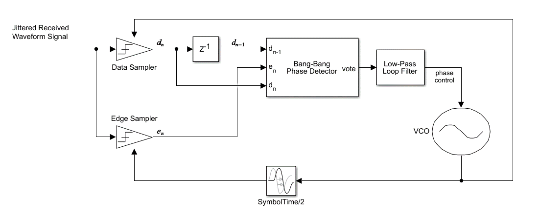
Phase Detector
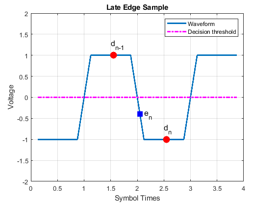
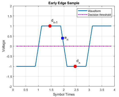
The Alexander or bang-bang phase detector samples the received waveform at the edge and middle of each symbol. The edge sample (en) and data samples (dn-1 and dn) are processed with some digital logic to determine if the edge sample, and thus the clock phase, is early or late. The edge sample, en, and data sample, dn, are separated by half of a symbol time.
Consider the waveform where a data transition has occurred, and both en and dn are below the decision threshold voltage. The binary values resolved from en and dn match, which indicates the clock phase is late.
Similarly, when the binary values resolved from en and dn-1 match, the clock phase is early.
Representing the binary output of the sampler by ±1, the behavior of the phase detector for NRZ or PAM4 modulation is summarized here:
| dn-1 | en | dn | Action |
|---|---|---|---|
| −1 | −1 | 1 | Clock phase is early. Shift phase to the right. |
| 1 | 1 | −1 | |
| −1 | 1 | 1 | Clock phase is late. Shift phase to the left. |
| 1 | −1 | −1 | |
| −1 | X | −1 | No action is necessary. |
| 1 | X | 1 |
For PAM3 modulation, the symbol levels are −0.5, 0, and 0.5. The default threshold levels (th) are ±0.25. The modified truth table thus become:
| dn-1 | en | dn | Action |
|---|---|---|---|
| −0.5 | en > −th | 0 | late |
| −0.5 | en < −th | 0 | early |
| −0.5 | en > 0 | 0.5 | late |
| −0.5 | en < 0 | 0.5 | early |
| 0 | en > th | 0.5 | late |
| 0 | en < th | 0.5 | early |
| 0 | en > −th | −0.5 | early |
| 0 | en < −th | −0.5 | late |
| 0.5 | en > th | 0 | early |
| 0.5 | en < th | 0 | late |
| 0.5 | en > 0 | −0.5 | early |
| 0.5 | en < 0 | −0.5 | late |
Driving the VCO directly from the phase detector output results in excessive clock jitter. To eliminate the jitter, the output of the phase detector is lowpass filtered by accumulating it in a vote. When the accumulated vote exceeds a specific count threshold, the phase of the VCO is incremented or decremented.
Recovering Clock Signal
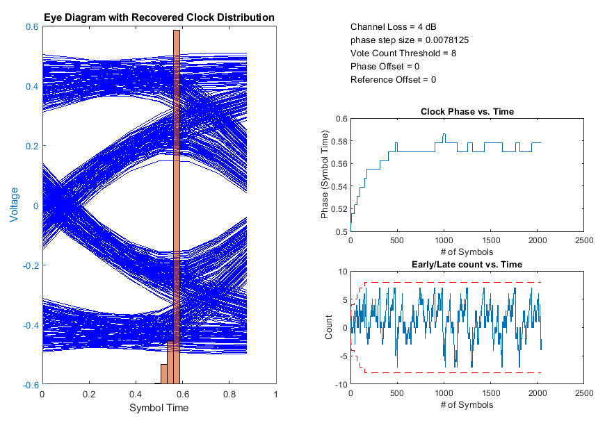
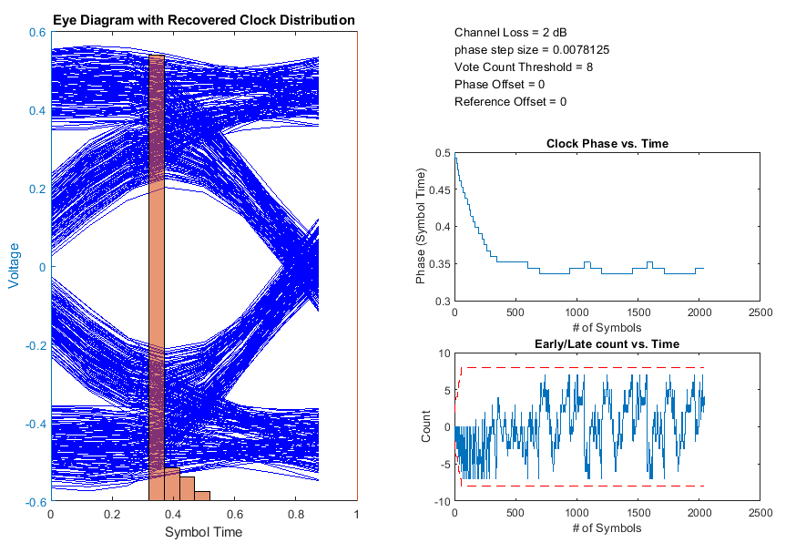
Recover the clock signal from a repeating pseudorandom binary sequence (PRBS9) nonreturn to zero (NRZ) signal. Consider the channel has 4 dB loss, the phase step size is , the vote count threshold is 8, and that there are no phase or reference offsets.
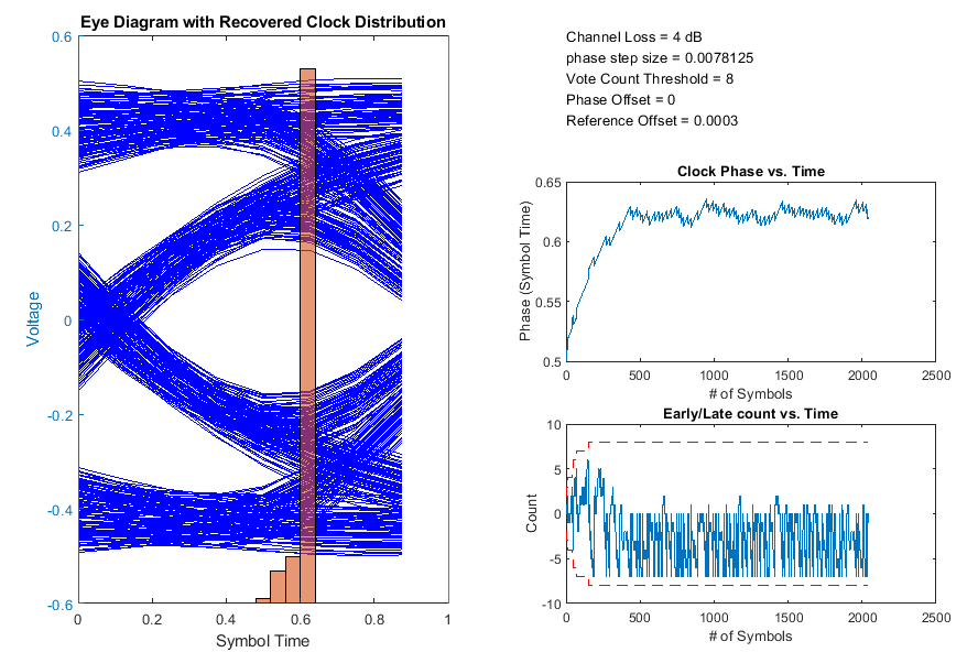
The baseline behavior is shown with the eye diagram and the resulting clock probability distribution function (PDF). The PDF is very near the center of the eye. The clock phase settles between a value of 0.5703 symbol time and 0.5781 symbol time. The dithering between the two values is a consequence of the nonlinear bang-bang phase detector and is the source of CDR hunting jitter. To reduce the magnitude of dithering, reduce the phase step size. To reduce the period of dithering, reduce the vote count threshold.
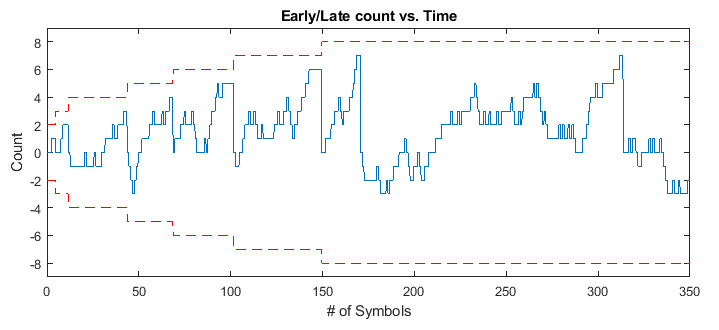
The output of the phase detector is accumulated in the early/late vote count. When the count exceeds the vote count threshold, the phase is incremented or decremented. To accelerate CDR convergence, the count threshold starts at 2, and each time the magnitude of the vote exceeds the threshold, the threshold is incremented until it reaches the maximum count. This figure shows the first 350 symbols of the early/late count (blue) and the threshold (dashed red line). Internal to the CDR block, the vote is incremented or decremented, checked against the threshold and then reset if necessary. The external vote value shown in figure below does not touch the threshold but is evident when the vote is reset to 0.
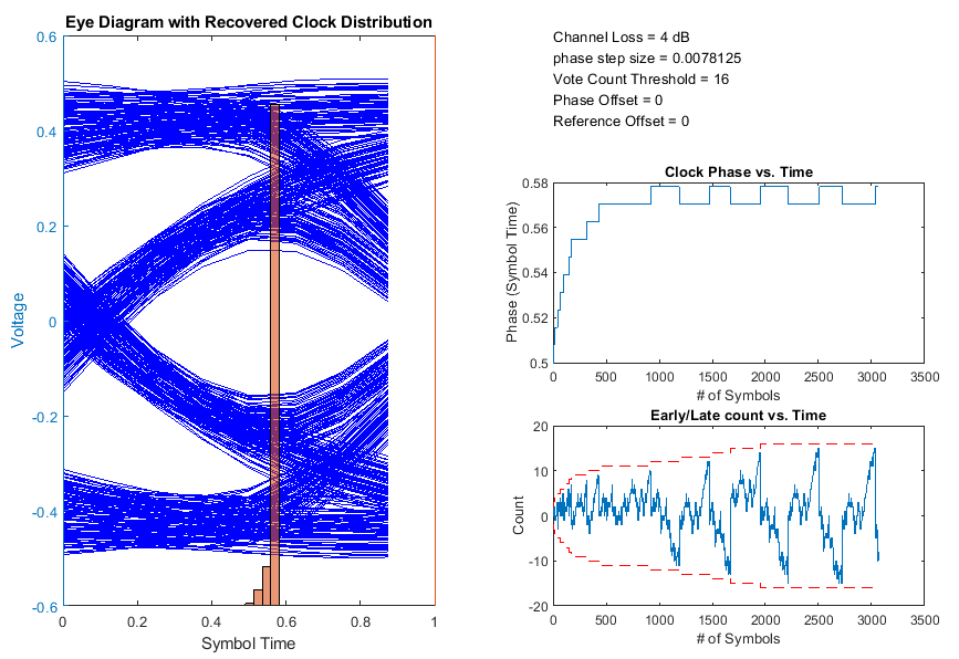
To show the clock converging to a different phase, change the channel loss to 2 dB. The clock phase now adapts to around 0.35 symbol time.
Increasing the vote count threshold to 16 results in a larger dithering period.
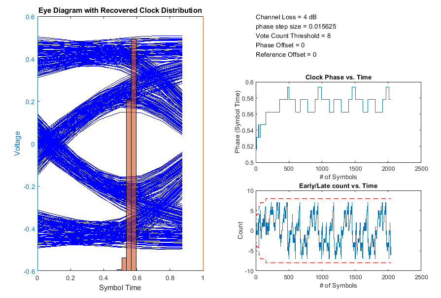
Increasing the phase step size to increases the dithering magnitude.
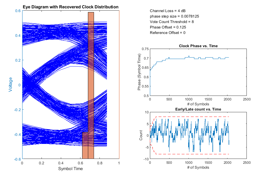
Manually shifting the data sampler location when the equalized eye does not display left/right symmetry can maximize the eye height. For example, shift the clock phase to the right by of a symbol time to shift the output clock phase from 0.57 symbol time to 0.7 symbol time.
You can also inject a small amount of reference clock frequency offset impairment to implement a more realistic CDR.
References
[1] Sonntag, J. L. and Stonick, J. "A Digital Clock and Data Recovery Architecture for Multi-Gigabit/s Binary Links." IEEE Journal of Solid-State Circuits, 2006.
[2] Razavi, B. "Challenges in the design high-speed clock and data recovery circuits." IEEE Communications Magazine, 2002.
See Also
serdes.CDR | serdes.DFECDR | DFECDR | CDR