Edge Detection and Image Overlay
This example shows how to design a video application with HDMI input and output. The example models an algorithm that detects the edges in the input video, overlays the edges on the input video, and outputs the modified video. The example simulates the design in Simulink® and deploys the design to hardware by using the SoC Builder tool.
This example uses the SoC Builder workflow. For an example of the same algorithm implemented and deployed by using the IP core generation workflow, see Developing Vision Algorithms for Zynq-Based Hardware. For information about these workflows, see SoC Generation Workflows.
Supported hardware platform:
AMD® Zynq® Ultrascale+ ZCU102 evaluation kit + FMC-HDMI-CAM mezzanine card
Modeling
In the top model, soc_edge_detection_top.slx, the FPGA logic is connected to the HDMI Rx and HDMI Tx blocks. The HDMI blocks represent the interface between the camera card and the FPGA. In simulation, the HDMI Rx block converts a video file to pixel-stream format.
open_system('soc_edge_detection_top')
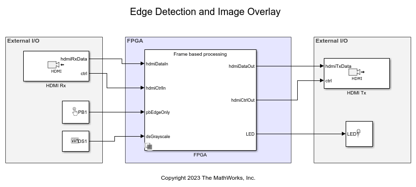
The FPGA subsystem has two options for Model Variant : Frame based processing and Pixel based processing. It also has a parameter that selects the frame resolution in the FPGA subsystem.
When you set Model Variant to Frame based processing, the FPGA subsystem links to the soc_edge_detection_fpga_frame.slx model that includes a frame-based edge detection algorithm. This version of the algorithm is for behavioral reference, and it does not support HDL code generation.
When you set Model Variant to Pixel based processing, the FPGA subsystem links to the soc_edge_detection_fpga_pixel.slx model that includes HDL-ready logic for the edge detection and overlay algorithm. This model uses Video Stream Connector blocks to represent an AXI4-Stream interface with your logic on the FPGA. The Edge Detection Wrapper subsystem includes the FPGA subsystem and a Video Stream FIFO block that implements a backpressure control signal for the output video stream.
open_system('soc_edge_detection_fpga_pixel')
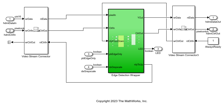
The pbEdgeOnly and dsGrayscale ports are intended to connect to a push button and DIP switch in hardware, respectively. The design also uses cThreshold and cAlpha parameters to control the behaviour of the edge detect and overlay algorithms. In the model, these parameters are declared as Constant blocks defined by workspace variables. The SoC Builder tool maps these parameters to registers.
Before opening the SoC Builder tool, the Model variant in the FPGA subsystem must be set to Pixel based processing.
Implement and Run on Hardware
You must have these products for this section:
HDL Coder™
SoC Blockset™ Support Package for AMD® FPGA and SoC Devices.
To implement the model on a supported SoC board use the SoC Builder tool. Open the mask of FPGA subsystem and set Model variant to Pixel based processing.
To open SoC Builder, in the Simulink toolstrip, on the System on Chip tab, click Configure, Build, & Deploy.
On the Setup screen, select Build model. Click Next.
On the Select Build Action screen, select Build, load, and run. Click Next.
On the Select Project Folder screen, specify the project folder. Click Next.
On the Configure FPGA Parameters screen, select Include processing system and Include AXI Manager IP for host-based interaction
On the Review Hardware Mapping screen, view the memory map by clicking View/Edit. Click Next.
On the Validate Model screen, check the compatibility of the model for implementation by clicking Validate. Click Next.
On the Build Model screen, begin building the model by clicking Build. An external shell opens when FPGA synthesis begins. Click Next.
On the Load Bitstream screen, click Next.
On the Connect Hardware screen, click Test Connection to test the connectivity of the host computer with the SoC board. Click Next to go to the Run Application screen.
The host computer can tune parameters by writing to AXI4-Lite registers within the algorithm IP core by using the generated interface script named gs_soc_hdmi_top_interface. The script includes this code that sets the cAlpha and cThreshold values to 0.5 and 7, respectively
writePort(hFPGA, "cAlpha", 0.5);
writePort(hFPGA, "cThreshold", 7);
To view the results from the design running on the board, connect an HDMI monitor to the output of the FMC-HDMI-CAM card.
See Also
HDMI Rx | HDMI Tx | Video Stream FIFO | Video Stream Connector