Architectural Design of a Low IF Receiver System
This example shows how to use the RF Blockset™ Circuit Envelope library to simulate the performance of a Low IF architecture with the following RF impairments:
Component noise
Interference from blocker signals
LO phase noise
Analog-to-digital converter (ADC) dynamic range
Component mismatch
Design variables in the RF portion of the model include explicit specification of gain, noise figure, IP3, input/output impedance, LO phase offset, and LO phase noise. Carrier frequencies for waveforms entering RF Blockset subsystems are specified in the Inport blocks. Design variables for the transmitter side of the RF interface include carrier frequency, modulation scheme, signal power, and blocker power level. Baseband design variables are number of bits and full scale range of the ADC.
System Architecture
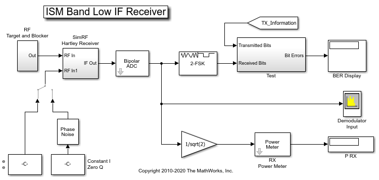
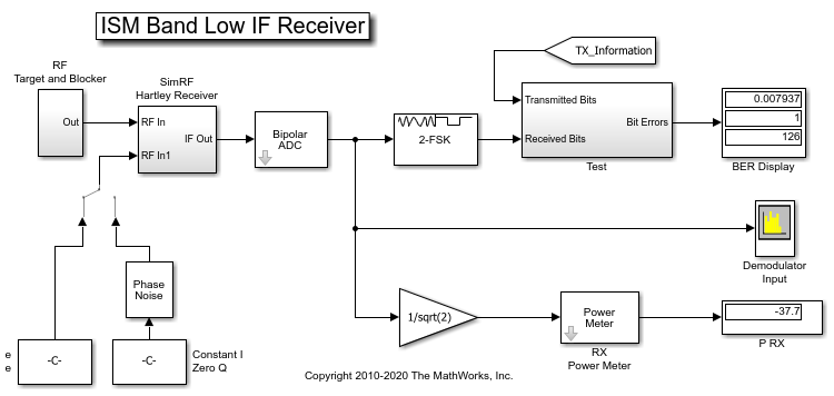
This model illustrates the design and simulation of an ISM Band Receiver. Primary subsystems include a digital transmitter, an RF receiver, an ADC, a phase noise block for noisy LO modeling, and a digital receiver. The remaining blocks are used for analysis.
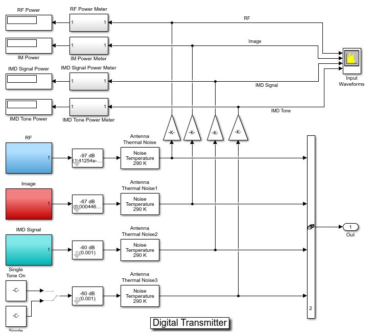
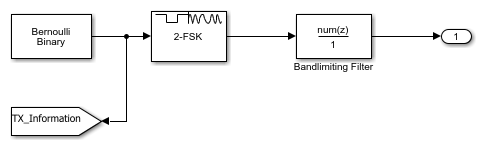
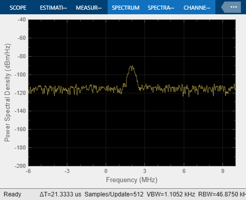
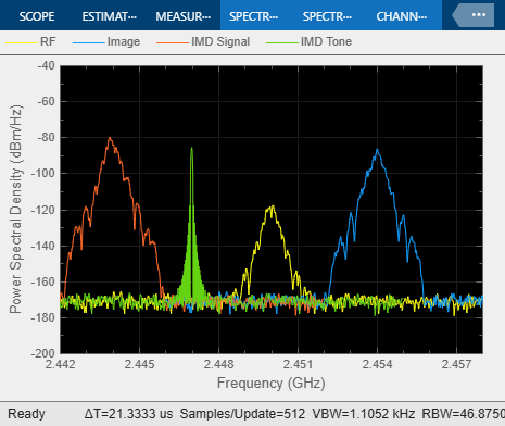
The digital transmitter consists of three FSK modulated waveforms and a high power tone. The three FSK waveform generators use a bandlimiting filter that suppresses the FSK sidebands below the expected thermal noise level. The target waveform at 2450 MHz has a 1 ohm referenced passband power level of approximately -70 dBm. Similarly defined image and intermodulation distortion (IMD) blocker waveforms have passband powers of approximately -40 dBm and -33 dBm, respectively. The IMD tone that couples with the IMD blocker to generate in-band IM3 products has a passband power of -33 dBm. Since the baseband processing defines the complex envelope waveforms, computing passband power requires the insertion of 1/sqrt(2) gain as shown in the design. An IF of 2 MHz can be inferred by inspecting the demodulator input signal spectrum, where a 2 MHz offset is specified for the display.
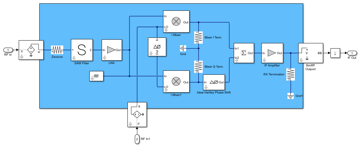
The Low IF receiver is comprised of a receive band SAW filter, a frequency conversion stage, an image rejection stage, and two gain stages. Resistors are used to model input and output impedances. Each nonlinear block has a noise figure specification. Power nonlinearities in the low noise amplifier (LNA), IF amplifier and mixers are specified by IP3. Image rejection is accomplished with a Hartley design, and single LO and phase shift blocks provide cosine and sine terms to mix with the I and Q branches, respectively. The summation block recombines the signals on the I branch and the phase-shifted Q branch. Image rejection quality can be controlled directly by setting a non-ideal phase offset in the Phase Shift block. To capture the RF, Image, IMD Signal and IMD Tone waveforms/spectra, choose the Fundamental tones to be 2450 MHz, 1 MHz and the Harmonic Order as 1 for the first tone and 8 for the second tone within the Configuration block. To model a thermal noise floor in the RF Blockset environment, the Temperature within the System Parameters section in the Configuration block is set to a noise temperature of 290.0 K.
The ADC is modeled using a 12-bit quantizer. The quantizer takes into account the full-scale and dynamic ranges of the ADC, properly modeling its quantization noise floor.
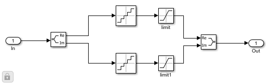
A digital receiver demodulates the waveform for bit error rate calculation. This noncoherent FSK receiver assumes perfect timing synchronization, such that each FSK pulse is integrated over one and only one symbol.
Running the Example
Running the example simulates a design that meets an uncoded BER spec of less than 1%. Modifications to the signals and component specifications in the receiver and ADC have a direct impact on the receiver performance. Manual switches enable you to:
Select a power level for the IMD blocker tone of -33 dBm or -45 dBm
Select an ideal or noisy LO.
Other possible changes to the design include:
Image rejection ratio (IRR) of the Hartley design. The IRR of the present design (dPhi=0.01 degrees) is -40 dB. For more information on calculating IRR, see the example
Measuring Image Rejection Ratio in Receivers (RF Blockset)Measuring Image Rejection Ratio in Receivers>.
Modulation schemes
Baseband filtering options
Signal power levels
Signal carrier frequencies
Noise figures
Non-linear gain parameters
Interstage matching
ADC bit length and full scale range
See Also
Topics
- RF Noise Modeling
- Circuit Envelope Simulation (RF Blockset)