Read and Write EEPROM Using SPI Blocks on Renesas RA Microcontrollers
R2026bThis example shows how to communicate with an SPI-based EEPROM using Renesas RA6 microcontrollers in Simulink. The example demonstrates two approaches for implementing SPI communication:
Read and write EEPROM data by using the SPI Controller Transfer block
Read and write EEPROM data by using the SPI Controller Transmit and SPI Controller Receive blocks
Both models write data to the EEPROM at a specified memory address, then read it back and display the result to verify correct operation.
Prerequisites
Before you begin,
Complete these tutorials:
Review the MCK-RA6T2 User's Manual.
Complete the Hardware Setup for Embedded Coder Support Package for Renesas RA Microcontrollers.
Required Hardware
Renesas RA microcontroller board
SPI-based EEPROM device
Jumper wires
USB cable
FTDI Friend (For example FTDI Friend USB TTL-232R 3.3V adapter)
RASC Configuration
Each example model includes a Renesas RA Smart Configurator (RASC) configuration file that defines the SPI peripheral setup, pin assignments, clock configuration, and FSP module stack. The RASC configuration is generated using FSP version 6.3.0 targeting the R7FA6M3AH3CFC device on the EK-RA6M3 board.
Common Configuration
Both configurations use:
Device: RA6M3 (R7FA6M3AH3CFC)
Core: Cortex-M4
FSP Version: 6.3.0
Board: RA6M3-EK
SPI Bitrate: 1 MHz
EEPROM Module Concepts
Memory Layout and Addressing
The Microchip 25XX080 8K SPI Bus Serial EEPROM module has 8Kbits of memory (1024 bytes) and requires 10 bits (A0 to A9) to address the entire memory space. The SPI protocol for the device requires a 16-bit address for data transmission.
Valid address range: 0x0000to0x03FF(0to1023accounting for 1024 bytes)Address transmission: 16-bit address is split into two bytes
High byte (MSB): Contains Don't Care bits (
A15toA10) and the two highest physical address bits (A9 andA8)Low byte (LSB): Contains the lower 8 physical address bits (
A7 toA0)
To address 0x0200:
Transmit MSB:
0x02(0b0000 0010)Transmit LSB:
0x00(0b0000 0000)
The memory is divided into 16-byte pages. Writes must not cross page boundaries in a single operation. When writing multiple bytes (for example, the address increments past 0bxxxx 1111), the internal address counter rolls over to the start of the same page, overwriting previous data. To write to contiguous memory across page boundaries, for each page, increment the address by 0x10 (16 decimal) and then perform a write operation.
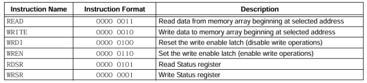
This table, from the Microchip 25XX080 8K SPI Bus Serial EEPROM datasheet, shows the module instruction set.
Write to EEPROM
To write to the EEPROM:
1. Set the write enable latch with the WREN instruction by completing this write enable sequence:
Drive chip select (CS) line low > Send 0x06 > Drive CS line high
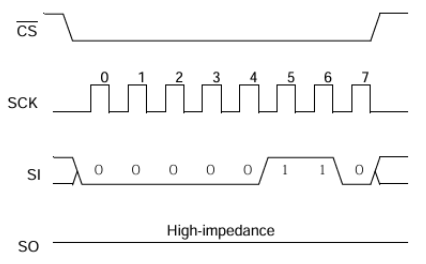
If you do not set the write enable latch (WEL) or toggle the CS line, a silent failure occurs.
2. Initiate a write operation with the WRITE instruction by completing this page write sequence:
Drive CS line low > Send 0x02 (WRITE) > Send 16-bit Address > Send Data (Max 16 bytes) > Drive CS line high after data byte is transferred
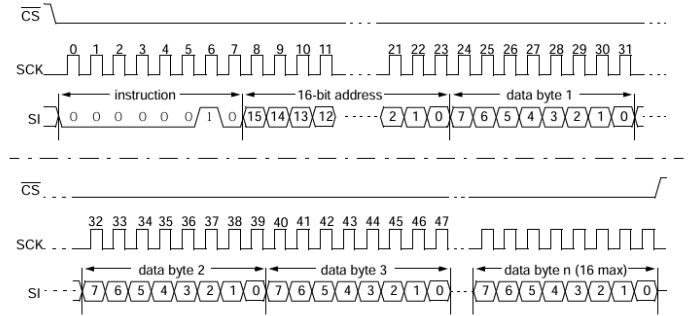
3. Trigger a write cycle.
To write data to memory, drive the CS line high after the least significant bit (D0) of the last most data byte has been clocked in. Otherwise, the write operation does not complete.
The Microchip 25XX080 8K SPI Bus Serial EEPROM datasheet mentions that the internal write cycle time (Twc) is a maximum of 5 ms and an attempt to read from a memory location is not possible during a write cycle.
The write enable latch (WEL) is automatically reset when the write cycle is completed.
Read from EEPROM
Initiate a data read from an address of the EEPROM after confirming that data was successfully written. You have two options for checking the status of a write operation:
Wait for a maximum of 5 ms of write cycle time.
Poll the Write-In-Process (WIP) bit in the Read Status Register (RDSR), which is at address 0x05.
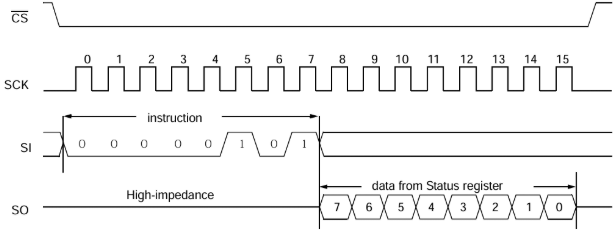
To poll the WIP bit:
Drive CS line low → Send
0x05(RDSR) → Send a dummy byte (0x00) to read the 8-bit register value.Check bit 0 (WIP). A value of 1, indicates Busy (the write is in progress). A value of 0, indicates Ready (the write is complete).
To read from the EEPROM, initiate this sequence of operations:
Drive CS line low.
Send
0x03(READ).Send 16-bit address (MSB then LSB).
Send dummy bytes to clock out data.
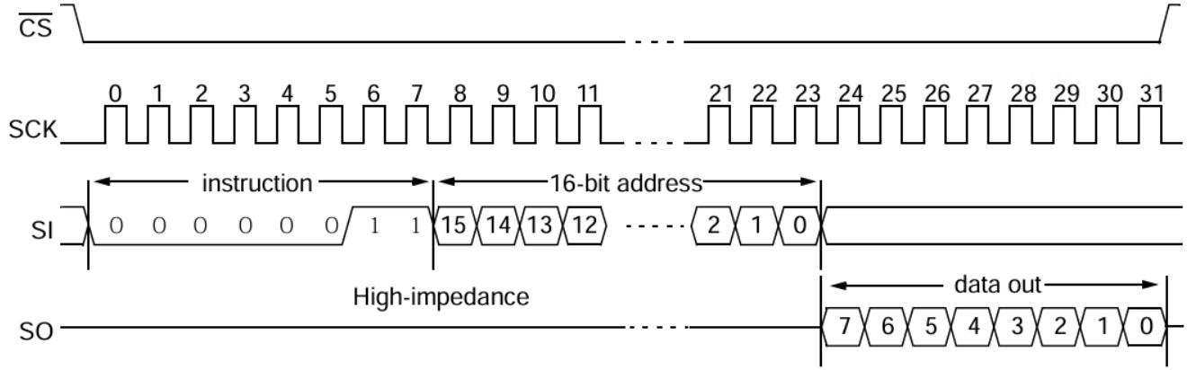
The address pointer automatically increments, allowing the entire array to be read in a single sequence,
Set Up Hardware Connections
Connect the Microchip 25AA080 SPI EEPROM device to the EK-RA6M3 board using SPI2.
EEPROM Pin | Signal | EK-RA6M3 Connection |
1 (CS) | Chip Select | SPI2 SSL |
2 (SO) | MISO | SPI2 MISO |
3 (WP) | Write Protect | 3.3 V |
4 (VSS) | Ground | GND |
5 (SI) | MOSI | SPI2 MOSI |
6 (SCK) | SPI Clock | SPI2 SCK |
7 (HOLD) | Hold | 3.3 V |
8 (VCC) | Supply | 3.3 V |
Use jumper wires to connect the EEPROM device to the EK-RA6M3 board. Ensure that the EEPROM and the board share a common ground.
When using an FTDI adapter for communication between the host computer and the Renesas RA6T2 target board, make the following connections.
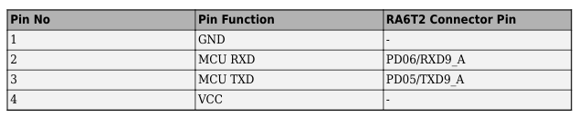
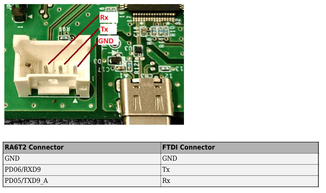
The Rx, Tx, and GND labels shown in red in the figure indicate the corresponding pins on the FTDI connector.
Read and Write EEPROM Using SPI Controller Transfer Block
This model (RA6M3spiEEPROMTransferController) uses the SPI Controller Transfer block, which performs simultaneous transmit and receive in a single SPI transaction. This approach simplifies the model by combining both data directions into one block.
1. Open the RA6M3spiEEPROMTransferController.slx Simulink model.
modelName = "RA6M3spiEEPROMTransferController";
open_system(modelName) 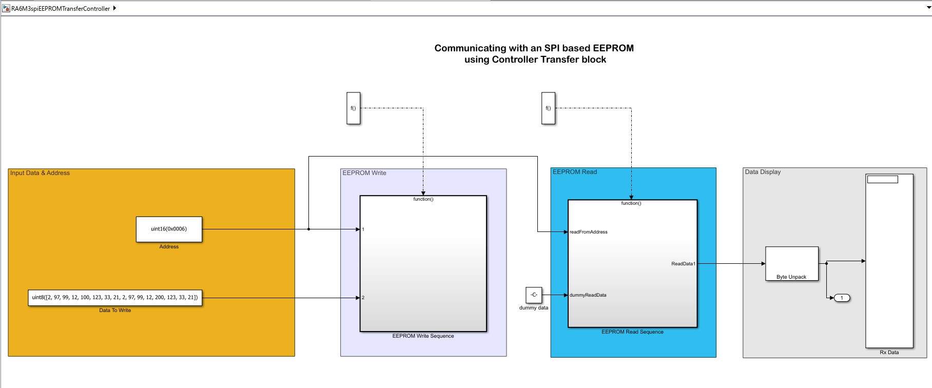
The top-level model has a similar structure to Model 1, with separate subsystems for write and read operations. Key differences include:
The address is set to
uint16(0x0006).Data is provided as
uint8array directly.A dummy data constant is used during read operations to clock data out of the EEPROM.
Block Configuration
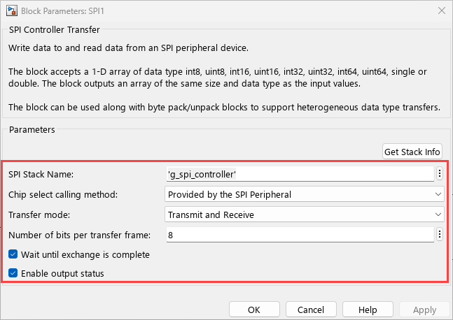
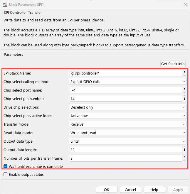
Open the SPI Controller Transfer block from the RA6M3spiEEPROMTransferController.slx example model. Configure the SPI module as shown below (SPI1 in this example):
EEPROM Write Sequence Subsystem
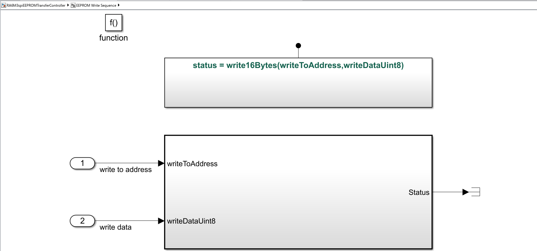
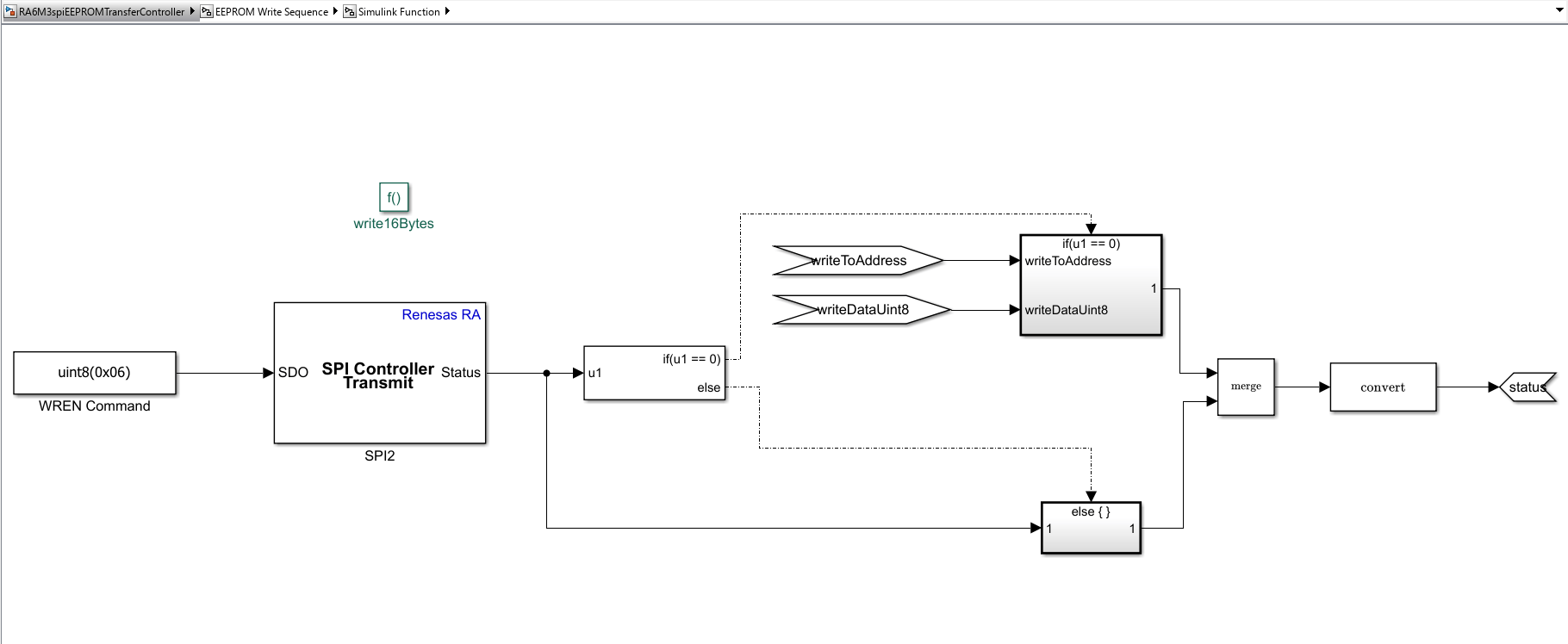
The write sequence in this model uses a Simulink Function (write16Bytes) that implements the complete write operation:
Sends the WREN command (
0x06) via the SPI Controller Transmit block (SPI2).Checks the transmit status.
If successful (
u1 == 0), proceeds to write the address and data bytes using an If-Action subsystem.Merges and converts the status output for error reporting.
Simulink Function: write16Bytes
Inside the Simulink Function, the WREN command is sent first. The status is checked using an If block, and upon success, the write address and data are passed to an If-Action subsystem that performs the actual page write via SPI.
EEPROM Read Sequence Subsystem
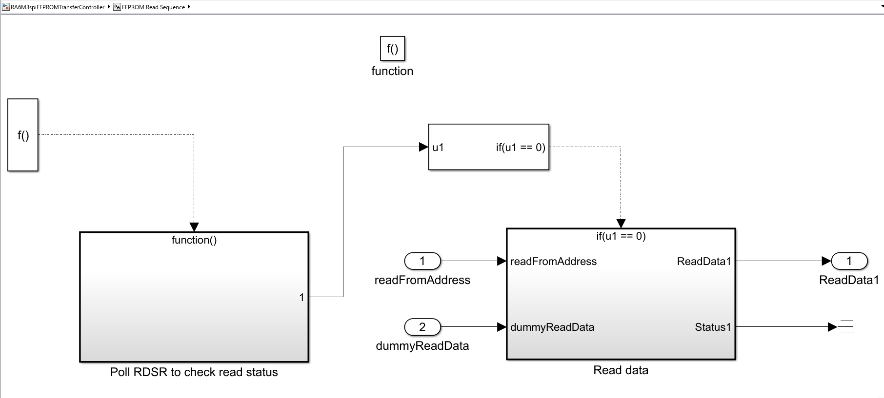
The read sequence uses two stages:
Poll RDSR to check read status — A function-call subsystem that verifies the EEPROM is ready.
Read data — Conditionally executes (when
u1 == 0) to read data from the specified address.
Read Data Subsystem
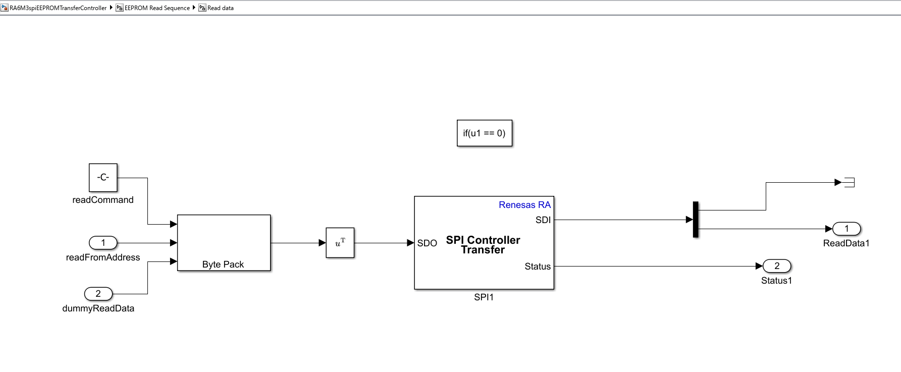
The Read data subsystem uses the SPI Controller Transfer block (SPI1) to simultaneously send the read command with the address (packed via Byte Pack) and receive the EEPROM response data. The SDO port sends the command/address, while the SDI port captures the returned data. A demux separates the received data (ReadData1) from the transfer status (Status1).
Read and Write EEPROM Data Using SPI Transmit and Receive Blocks
This model (RA6M3spiEEPROMTransmitReceive) uses separate SPI Controller Transmit and SPI Controller Receive blocks. This approach provides granular control over each phase of the SPI transaction.
1. Open the RA6M3spiEEPROMTransmitReceive.slx Simulink model.
modelName = "RA6M3spiEEPROMTransmitReceive";
open_system(modelName) 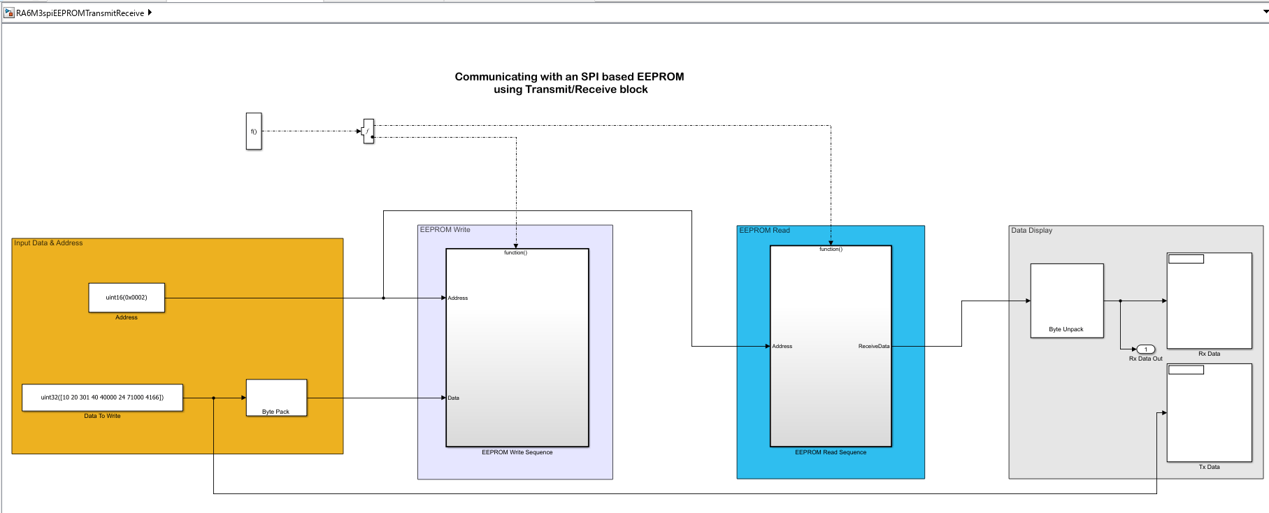
The top-level model consists of four main sections:
Input Data & Address — Defines the EEPROM write address (
uint16(0x0002)) and the data payload to write.EEPROM Write — Subsystem implementing the write sequence with write enable and status polling.
EEPROM Read — Subsystem implementing the read sequence to retrieve stored data.
Data Display — Byte Unpack and output ports to display received data.
Block Configuration
Open the SPI Controller Transfer block from the RA6M3spiEEPROMTransmitReceive.slx example model. Configure the SPI module as shown below (SPI1 in this example):
EEPROM Write Sequence Subsystem
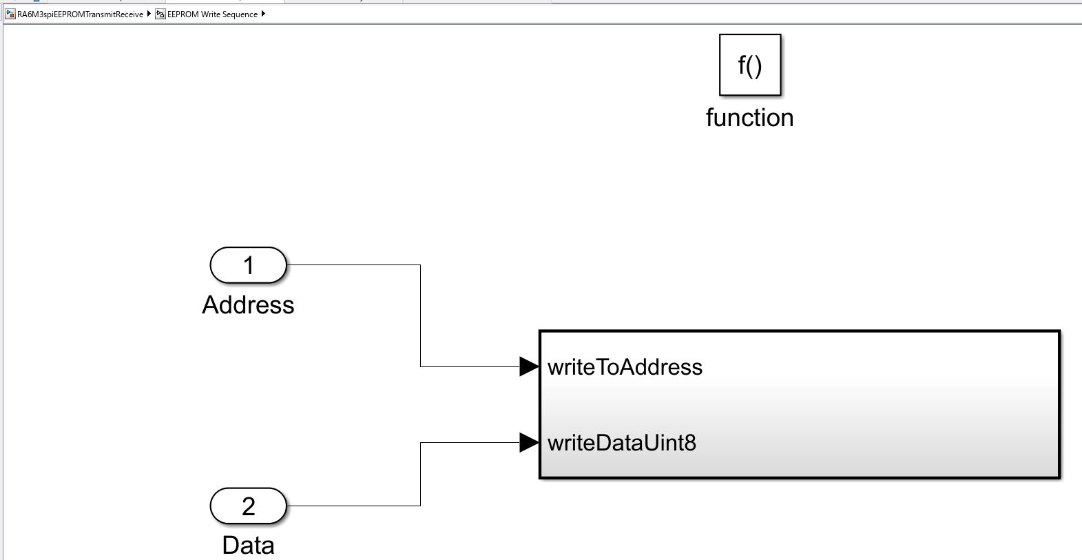
The write sequence subsystem accepts the target address and data as inputs. It uses a Simulink function to orchestrate the WREN command, followed by the actual page write operation. The subsystem uses a Renesas RA SPI Controller Transmit block to send the write command, address, and data bytes.
Write Cycle Status Polling
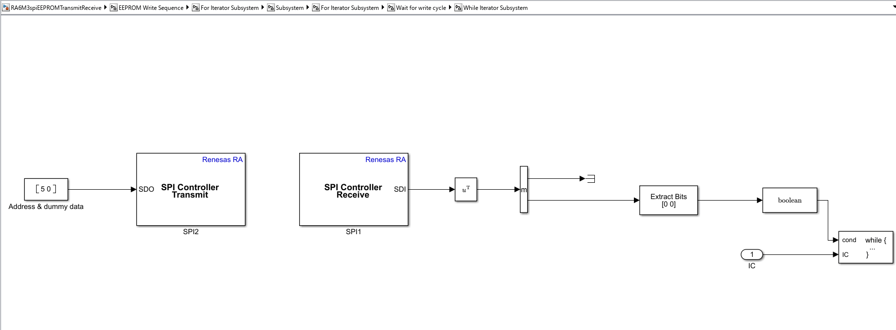
After initiating a write, the model polls the EEPROM's status register by sending the RDSR command via SPI Controller Transmit (SPI2) and reading the response via SPI Controller Receive (SPI1). The WIP bit (bit 0) is extracted and used as a while-loop condition to wait until the internal write cycle completes.
EEPROM Read Sequence Subsystem
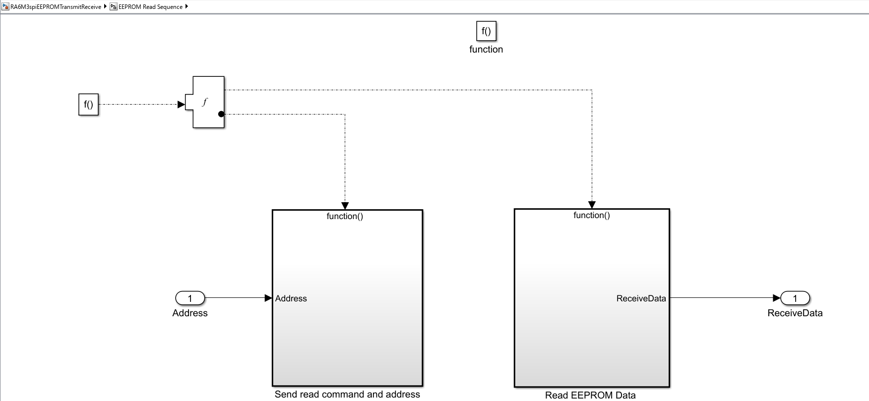
The read sequence is implemented using two sequential function-call subsystems:
Send read command and address — Transmits the READ opcode (
0x03) and the 16-bit address using the SPI Controller Transmit block.Read EEPROM Data — Receives the data bytes returned by the EEPROM via the SPI Controller Receive block.
Send Read Command and Address Subsystem
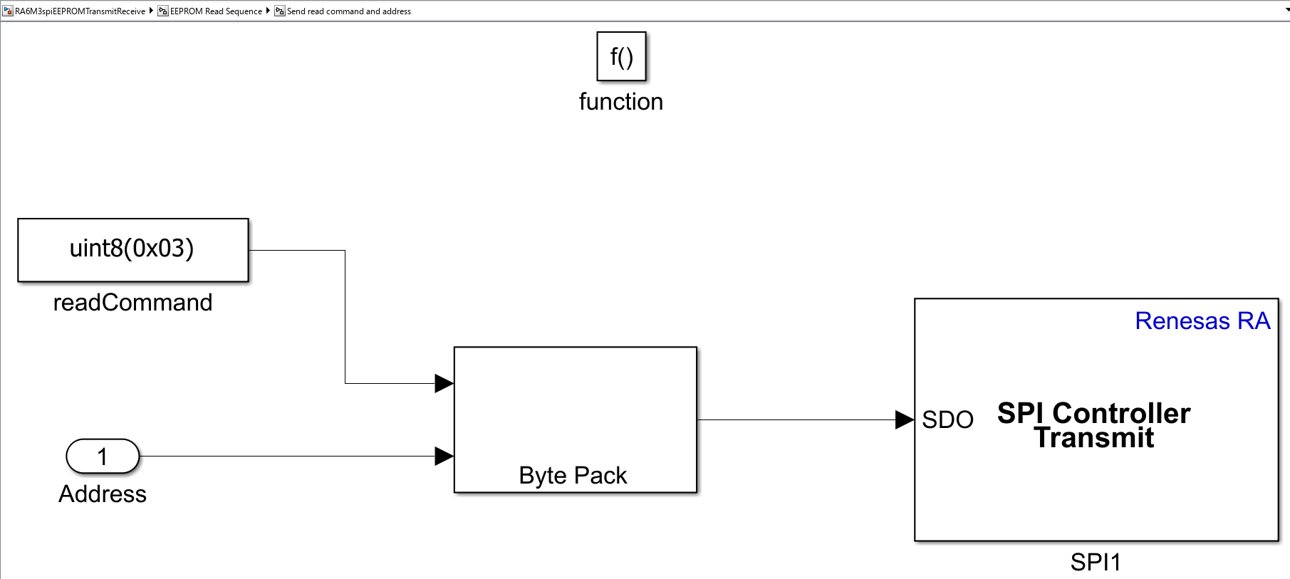
This subsystem packs the read command (0x03) and the 16-bit memory address into a byte array using the Byte Pack block. The packed data is transmitted via the Renesas RA SPI Controller Transmit block on SPI1.
Monitor and Tune the Model on Hardware
In the Simulink model, click Hardware tab and then click Monitor & Tune.This deploys the model to the target hardware.

2. Observe the receive display in the model.
3. Verify that the data read from the EEPROM matches the data written to the EEPROM.
Other Things to Try
Change the EEPROM start address and verify that the model reads from the new location.
Modify the input data vector and observe the updated receive data.
Compare the SPI Controller Transfer workflow with the SPI Controller Transmit/Receive workflow to understand how the same EEPROM protocol maps to two different block-level implementations.
If your EEPROM device has a smaller page size than the write data payload, update the write logic to split transactions on page boundaries, because the reference EEPROM behavior wraps writes within a page if a single write crosses the boundary.

