Getting Started with RH850 TSG3
This topic introduces the RH850 TSG3 (Timer for Smart Gate Drive 3) motor control timer and explains how it supports PWM generation and synchronized ADC triggering in Simulink-based workflows. It is designed to support advanced PWM generation, timing control, and synchronized ADC triggering, which are essential for digital power conversion and motor control applications.
The TSG3 blocks in Simulink represent the PWM and timing hardware, while AUTOSAR MCAL configuration defines how the TSG3 peripheral is initialized and mapped to physical pins on the RH850 target. This separation lets you focus on control algorithms in the model and rely on MCAL for correct, portable hardware configuration.
This topic assumes that PWM channels, timer configuration, ADC trigger routing, and pin multiplexing have been defined in the AUTOSAR MCAL configuration using Vector DaVinci Configurator. The TSG3, Port, and ADC MCAL modules must be configured coherently so that PWM outputs are routed to physical pins and ADC triggers are generated at the intended timing points.
The Simulink TSG3 blocks are constrained by the MCAL configuration. Unsupported channel mappings or missing pin configuration in the Port module prevent PWM signals from reaching the hardware pins.
See Configuring MCAL Modules Using DaVinci for information to create and export MCAL configuration data required by TSG3-based PWM and synchronized ADC workflows.
Prerequisites for Using the TSG3 Output Block
To generate PWM signals using the TSG3 Output block, you must complete all of the following configurations:
Model Configuration (Configset – TSG3 settings)
Configure the TSG3 instance, carrier frequency, duty-cycle update event (peak/valley), dead time, and ADC trigger events under:
In Configuration Parameters dialog box, navigate to Hardware Implementation > Target Hardware resources > TSG3.
MCAL Configuration (CDF / DaVinci)
Enable and configure the TSG3 peripheral in the MCAL configuration (CDF ARXML). This defines the PWM channels, operating mode, and trigger routing used by the generated code.
Port (Pin) Configuration (CDF / DaVinci)
Map the TSG3 PWM outputs to physical MCU pins using the Port module in the CDF configuration. Without correct pin multiplexing, PWM signals are generated internally but will not appear on the device pins.
Model-Level Block Configuration
In the TSG3 Output block, select the same TSG3 instance (for example, TSG30 or TSG31) that is enabled in the Configuration parameters and MCAL configuration.
The input duty vector must match the number of configured PWM phases (u, v, w).
What Is TSG3 Used For?
TSG3 is primarily used in applications that require deterministic, high‑resolution PWM waveforms and accurate coordination between switching events and signal sampling. Typical use cases include:
Motor control (BLDC, PMSM, induction motors).
Power converters (DC‑DC, DC‑AC, AC‑DC).
Servo drives and traction inverters.
Grid‑connected inverters and active front‑end converters.
In these systems, PWM generation, ADC trigger timing, and fault handling must be tightly coupled. TSG3 integrates these capabilities in a single hardware block, reducing CPU load and improving real-time determinism.
Key Capabilities of TSG3
The TSG3 module provides hardware support for timing and synchronization tasks that are performance-critical in motor control and power electronics:
High‑resolution timer counter for precise PWM timing
Support for high‑throughput PWM (HT‑PWM) with 0–100% duty cycle
Multi‑phase PWM generation for three‑phase motor control
Configurable dead‑time insertion for safe gate driving
Hardware‑synchronized ADC trigger generation
Fail‑safe mechanisms to force outputs to a safe state on faults
Depending on the RH850/U2A device variant, one or two TSG3 instances (for example, TSG30 and TSG31).
Where is TSG3 Used in the Workflow
TSG3 is intended for applications that require deterministic, high-resolution PWM waveforms and precise coordination between switching events and signal sampling. Typical use cases include motor drives and power conversion systems in which PWM timing directly affects control stability and measurement quality.
Control logic is designed and simulated in Simulink.
TSG3 blocks represent the PWM and timing hardware in the model.
MCAL configuration defines how the TSG3 peripheral is initialized on the target hardware.
Code generation maps the Simulink model to the RH850 TSG3 peripheral using AUTOSAR MCAL services.
This separation allows you to focus on control behavior at the model level while relying on MCAL to handle low‑level hardware configuration and portability.
End-to-End Workflow: From Model to Hardware
This workflow connects Simulink blocks, Configuration parameters, and MCAL configuration into a single, coherent setup:
Configure TSG3 in Model Settings (Configset)
Select the TSG3 instance (TSG30/TSG31), set the PWM carrier frequency, update timing (peak/valley), dead time, and optional ADC trigger events.
Configure TSG3 and Pins in MCAL (CDF / DaVinci)
Enable the TSG3 peripheral and map PWM outputs to physical pins using the Port module.
If ADC triggering is enabled, map the TSG3 trigger to the correct ADC instance.
Configure the TSG3 Output Block
Select the same TSG3 instance as in the Configset and provide a 3-element duty vector for u, v, and w phases.
Generate Code and Run on Target
Code generation maps the Simulink model to the configured TSG3 hardware through AUTOSAR MCAL.
Reload Timing and Duty Update Behavior
Peak/Valley Selection:
The Reload duty cycle counter event and Update duty cycle event parameters control when new duty values take effect within the PWM period.
This is critical for minimizing current ripple and measurement noise in motor-control applications.
Cross-Triggering with ADC
The ADC instance that receives the trigger is defined in the MCAL (CDF) configuration. Ensure that:
The selected ADC trigger source in the TSG3 configuration matches the ADC instance used by the ADC blocks in the model.
MCAL Configuration for a TSG3 Workflow
A valid TSG3 workflow requires coordinated configuration across multiple MCAL modules. Each module configures a different layer of the signal path, from PWM generation to pin routing.
TSG3 Configuration
Defines PWM channels, timer behavior, and trigger generation used by the Simulink TSG3 blocks.
Configure this in DaVinci under the TSG3 (or GPT/TSG) MCAL module. Key elements include:
Selection of the TSG3 instance (for example, TSG31)
PWM channel selection and operating mode
Timer base configuration and PWM carrier settings
Trigger generation for synchronized ADC sampling (if used)
These settings determine how the TSG3 hardware behaves at run time and constrain what the Simulink TSG3 blocks can generate.
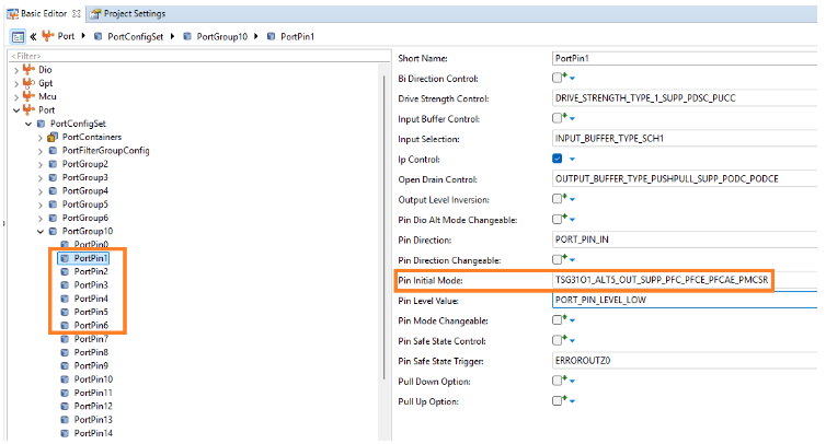
Port Module Configuration
Defines which physical pins are assigned to TSG3 outputs and how they behave electrically (alternate function, direction, drive strength).
Configure this in DaVinci, under Port -> PortConfigSet -> PortGroupX -> PortPinY. Typical settings include:
Pin initial mode set to the appropriate TSG3 alternate function
Pin direction set to output
Electrical characteristics such as drive strength and buffer type

Without correct Port configuration, the TSG3 PWM signals are generated internally but never reach the physical pins.
Common Problems TSG3 Helps Solve
TSG3 is designed to address several recurring challenges in motor‑control and power‑electronics systems:
Generating PWM signals with precise duty cycle and fixed carrier frequency
Keeping multiple PWM phases aligned and synchronized
Sampling currents or voltages at the correct electrical instant
Avoiding noisy measurements during switching transitions
Forcing PWM outputs to a known safe state during fault conditions
By handling these tasks in hardware, TSG3 reduces CPU load and improves execution.
See Also
Configuring MCAL Modules Using DaVinci | Control Onboard LED7 Brightness Using TSG3 Blocks on Renesas RH850 Microcontrollers