Serial Link Design
The Serial Link Designer app provides a dedicated system-level design and analysis environment for multi-gigabit serial links. Capture your serial link designs graphically and experiment with different physical layout and equalization strategies to predict how design alternatives affect operating margins and the bit error rate (BER) of the link. Use network characterization to model the behavior of the unequalized analog network. This enables quick evaluation of the analog channel design for different trade-offs. Predict the end-to-end behavior of the link using SerDes equalization techniques and clock recovery models obtained by statistical and time-domain analysis. Determine the effect of aggressor signals on overall BER of the channel using crosstalk analysis.
Use the Serial Link Designer app to configure high speed serial links. Set simulation parameters, specify corner conditions, and define stimulus patterns. Set up pre-layout analysis to run SPICE, network characterization, statistical and time domain simulations to analyze your custom serial links. View and interpret the results using the Signal Integrity Viewer app. You can also set up and analyze the post-layout PCB database of your serial link design if you have a license for RF PCB Toolbox™. You can modify the stackup and padstack models and customize vias and see how the changes impact your design.
Categories
- Serial Link Design Concepts
Learn the basics of serial link design projects using the Serial Link Designer app
- Configure Serial Link Projects
Configure serial link projects for simulations
- Pre-Layout Analysis of Serial Link Projects
Analyze serial link projects before designing board layouts
- Post-Layout Verification of Serial Link Projects
Verify the layout design of your system against design guidelines or specification rules
- Scripting in Serial Link Projects
Use MATLAB scripting commands to control the Serial Link Designer app
- Visualize and Interpret Serial Link Project Analysis Results
Visualize and interpret the network characterization and statistical and time domain analysis results
Featured Examples
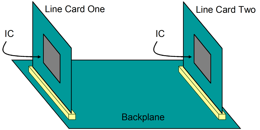
Analyze Backplane with Line Cards
Analyze a serial link consisting of a backplane and two line cards with the Serial Link Designer app. You can model the SerDes drivers/receivers, capture a topology for analysis, run network characterization, and evaluate the impact of different solution space variables on your design's performance.
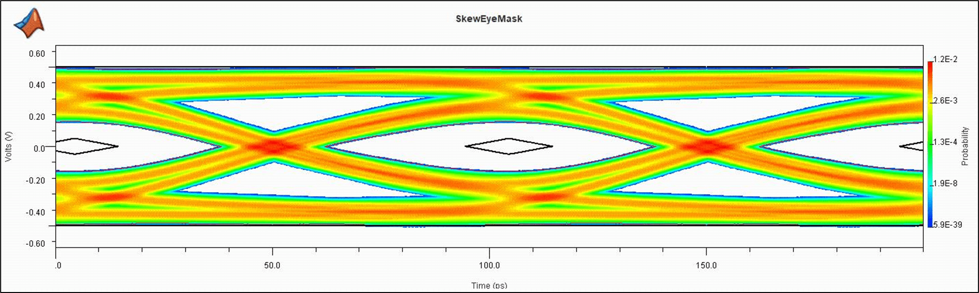
Creating Compliance Masks in Serial Link Designer
Create compliance masks and apply them to the simulation results in the Serial Link Designer app. The masks used in the Serial Link Designer app are defined in the rules file. Rules files are text files that define the mask limits for a parameter, or parameters in the channel simulation results. These are user created files that can be applied as eye masks or network loss characteristics. The file extension of a rules file must be “.rules” so that the Serial Link Designer app can recognize it as a mask file. The file must also be located in the <Project_Directory>\si_lib\rules\ directory of the project.
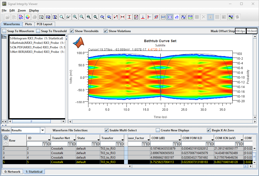
Channel Operating Margin (COM) for Serial Link
Use the channel operating margin (COM) metric within a Serial Link Designer project that has an interface that operates at 100 GT/s per Lane with NRZ modulation. COM is a figure of merit for a passive channel that gives you insight into the quality of the channel design. To calculate COM, use the ratio of signal amplitude factors to noise amplitude factors. Several factors such as channel bit rate, insertion loss, return loss, cross-coupling, transmitter and receiver equalization, and IC package models are applied to determine COM. COM is a valuable part of channel design methodology in general and is required for compliance in some applications such as IEEE 802.3 and OIF CEI standards. For more information on how to calculate and set up COM and how to interpret COM results, see Channel Operating Margin (COM).
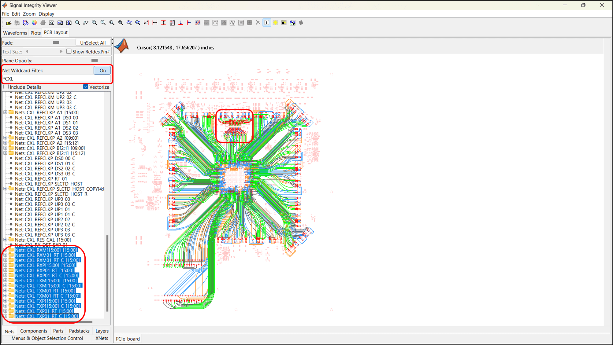
Post-Layout Verification of PCIe 5.0 Allegro Board
Analyze a printed circuit board created in Cadence® Allegro, analyze multiple PCIe 5.0 lanes to determine which will have open or valid eye diagrams, and how to isolate and diagnose lanes with closed eye diagrams by back drilling vias. You can import the board, set it up for simulation by assigning parts, use EBD files for loopback boards, simulate at PCIe 5.0 data rate of 32 Gbps, and finally debug to fix a closed eye diagram.
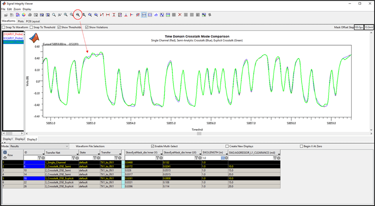
Crosstalk Analysis with Serial Link Designer
Perform pre-layout crosstalk analysis using the Serial Link Designer app.
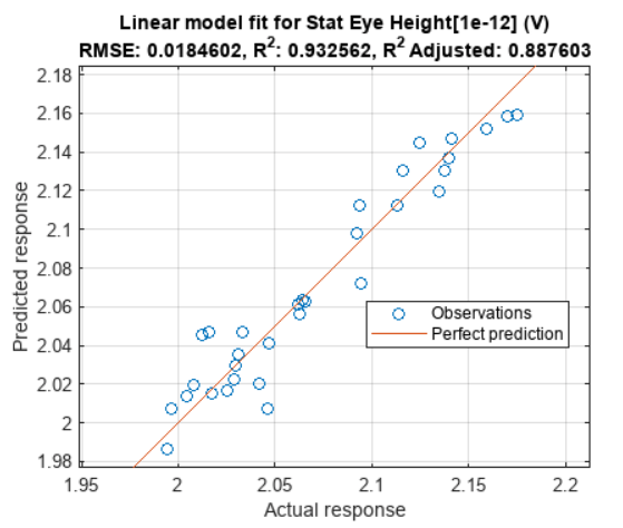
Explore Signal Integrity Interface with Design of Experiments and Response Surface Modeling
Setup and create a Design of Experiments (DOE) using the MATLAB® scripting interface in the Signal Integrity Toolbox™. You can simulate dozens of cases and use the Statistical and Machine Learning Toolbox™ to fit and analyze a linear model.