GPS Acquisition and Tracking Using AMD RFSoC Device
This example shows how to deploy a global positioning system (GPS) acquisition and tracking algorithm on an AMD® ZCU111 RFSoC Evaluation Board, using SoC Blockset™. The example builds on the GPS HDL Acquisition and Tracking Using C/A Code (Wireless HDL Toolbox) example, adding the infrastructure and connectivity around the receiver to implement the design on hardware. You can use MATLAB® to control, analyze and verify the behavior of the design.
Supported Hardware Platforms
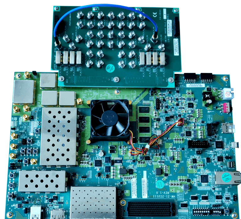
AMD Zynq UltraScale+ RFSoC ZCU111 Evaluation Kit + XM500 Balun card.
System Architecture
The example shows the workflow for designing, simulating, and deploying the GPS acquisition and tracking algorithm on the hardware. This figure shows the conceptual overview of the example.
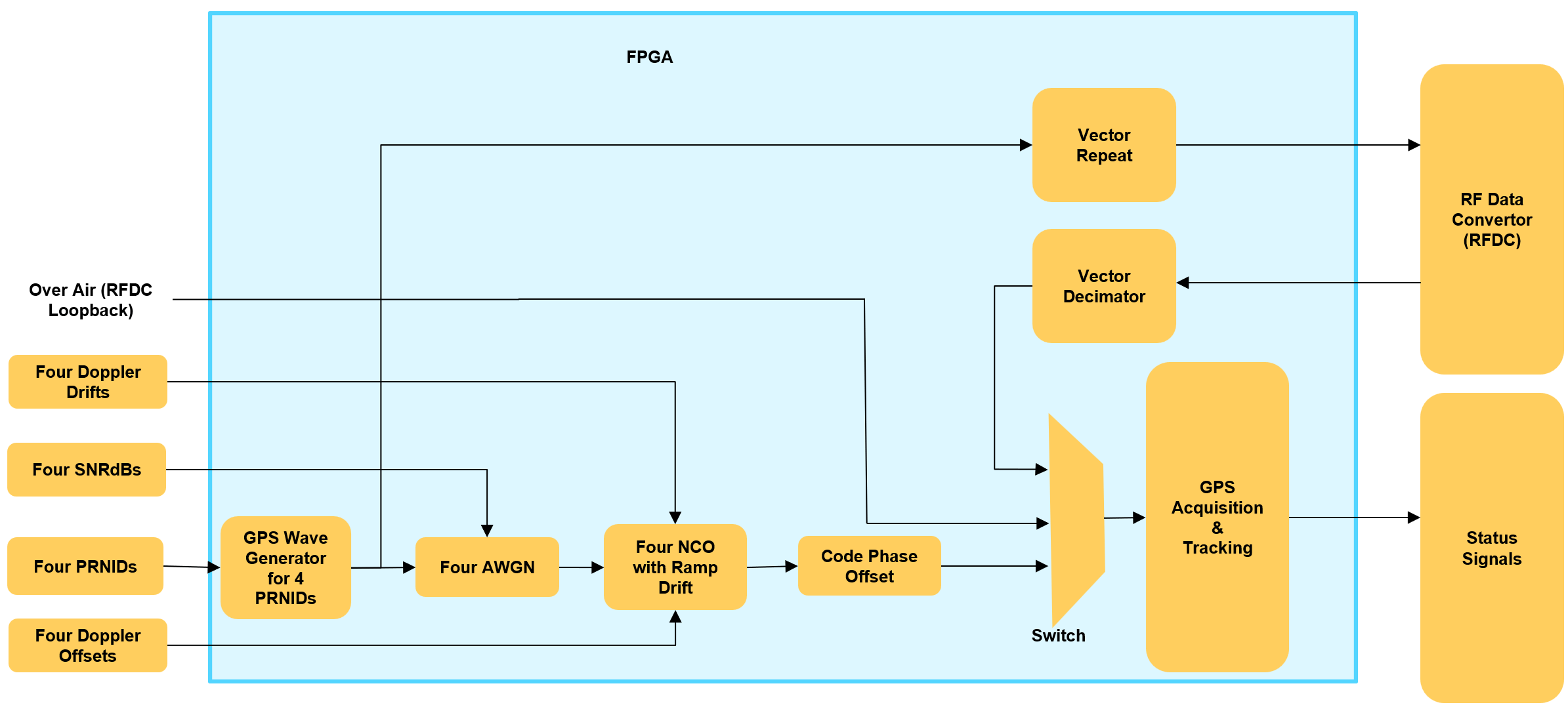
The acquisition and tracking feature in the GPS receiver performs high-speed signal processing tasks and makes it well-suited for FPGA implementation on the programmable logic (PL) of the radio platform. To implement this algorithm on the PL, the example uses the Simulink hardware model from the GPS HDL Acquisition and Tracking Using C/A Code (Wireless HDL Toolbox) example as model reference. The example is configured for four satellites and includes an LUT-based GPS waveform generator equipped with a C/A code generator. This example also has an internal channel to apply carrier frequency offset (CFO), carrier frequency drift (CFD), and an HDL-based additive white Gaussian noise (AWGN) channel from the HDL Implementation of AWGN Generator (Wireless HDL Toolbox) to verify the system performance against RF impairments.
Design Using SoC Blockset
Create an SoC model soc_GPS_top as the top model and set the Hardware Board parameter to Xilinx Zynq UltraScale+ RFSoC ZCU111 evaluation kit. The top model includes FPGA model soc_GPS_fpga and processor model soc_GPS_proc, which are instantiated as model references. The top model also includes AXI4-Stream to Software block that shares the external memory between the FPGA and the processor.
Create an SoC model soc_GPS_hwtop to act as the top-level model for simulating a hardware algorithm with a static configuration. This model includes the FPGA model soc_GPS_fpga.
RF Data Converter Configuration
An RFSoC device has its RF Data Converter (RFDC) connected to the PL. To configure the analog to digital converter (ADC) and digital to analog converter (DAC) settings, use the RFDC block. The block provides an interface to the AMD RFDC IP in Simulink for modeling a GPS system designed for implementation on an AMD RFSoC device.
You must perform sample rate conversion steps to convert to and from the sample rates required by the RFDC interface. The DAC and ADC operate at a sample rate of 3145.728 MSPS. The RFDC uses interpolation and decimation modes to achieve a stream clock rate of 196.608 MHz at the interface between the RFDC and the FPGA design. Use this sample rate at the interface to the FPGA from the RFDC as the FPGA clock rate, because it is the highest sample rate required on the FPGA.
To meet the 196.608 MHz clock rate, configure the RF Data Converter block according to the settings described here.
Set the DAC and ADC sample rates to
3145.728MSPS. DAC 2 from tile 1, and ADC 0 from tile 0 are used, corresponding to connections J5 and J4 on the XM500 balun card.Choose the values of Interpolation mode (xN), Decimation mode (xN), and Samples per clock cycle parameters such that the effective clock cycle (sample rate) for the GPS algorithm FPGA is the desirable value. For this example, the desired value is 196.608 MHz. This value is calculated and displayed on the block mask as the Stream clock frequency (MHz) parameter after you click Apply.
Set the Decimation mode (xN) parameter to
4. The effective sample rate after vector decimation is 786.432 MHz.Set the Samples per clock cycle parameter to
4to get the clock rate (baseband sample rate) to 196.608 MHz.Set the NCO frequency parameter for the DAC and ADC mixers to
0.860GHz.
Similarly, in the DAC tab, set the Interpolation mode (xN) parameter to 4 and the Samples per clock cycle parameter to 4. With these settings, the Stream clock frequency parameter is (3145.728)/(4*4) = 196.608 MHz.
Hardware Logic Design
The FPGA model soc_GPS_fpga consists of four subsystems: Vector Repeat (connected to the DAC part of the RFDC block), Vector Decimation (connected to the ADC part of the RFDC block), GPS Waveform 4 satellites, and GPS Acquisition and Tracking.
The GPS Waveform 4 Satellites subsystem has an LUT-Based GPS waveform generators for 4 satellites, 4 AWGN subsystem and 4 NCO with Ramp Doppler Rate subsystem for each of the satellites. The AWGN subsystem uses the AWGN generator from the HDL Implementation of AWGN Generator (Wireless HDL Toolbox) example. The NCO with Ramp Doppler Rate subsystem performs the CFO and CFD insertion using the NCO (DSP HDL Toolbox) block.
In the transmit path, the LUT-Based GPS waveform generator sends the samples to the RF Data Converter block. The samples are initially repeated by a factor of 6, and then the Vector Repeat subsystem further repeats the input samples by a factor of 4.The design then groups these samples into vectors of four and sends them to the RF Data Converter block to operate at a clock rate of 196.608 MHz.
In the receive path, the Vector Decimator subsystem receives the packed four samples with a clock rate of 196.608 MHz from the RF Data Converter block. The Vector Decimator subsystem decimates the input vector samples by a factor of 4 and further decimates the resulting scalar samples by a factor of 6. It then sends them to the GPS Acquisition and Tracking subsystem, which operates at a sample rate of 32.768 Msps with an oversampling factor of 6, as required by the GPS Acquisition and Tracking subsystem for its processing.
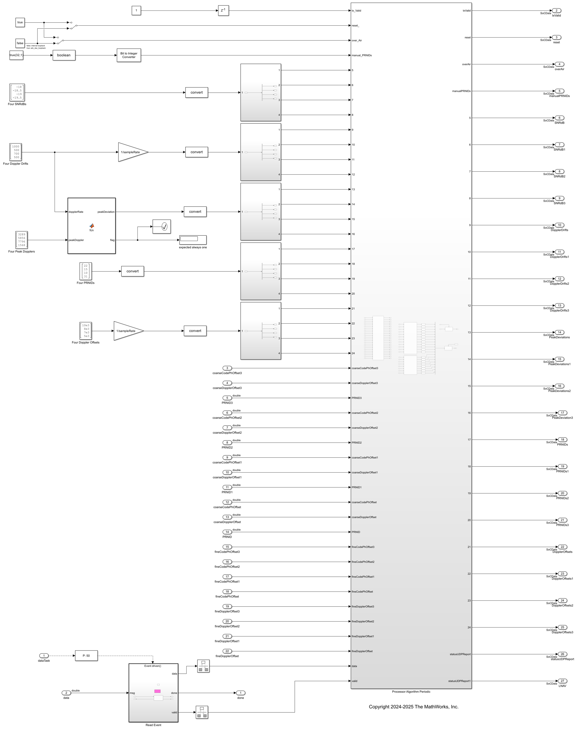
Processor Logic Design
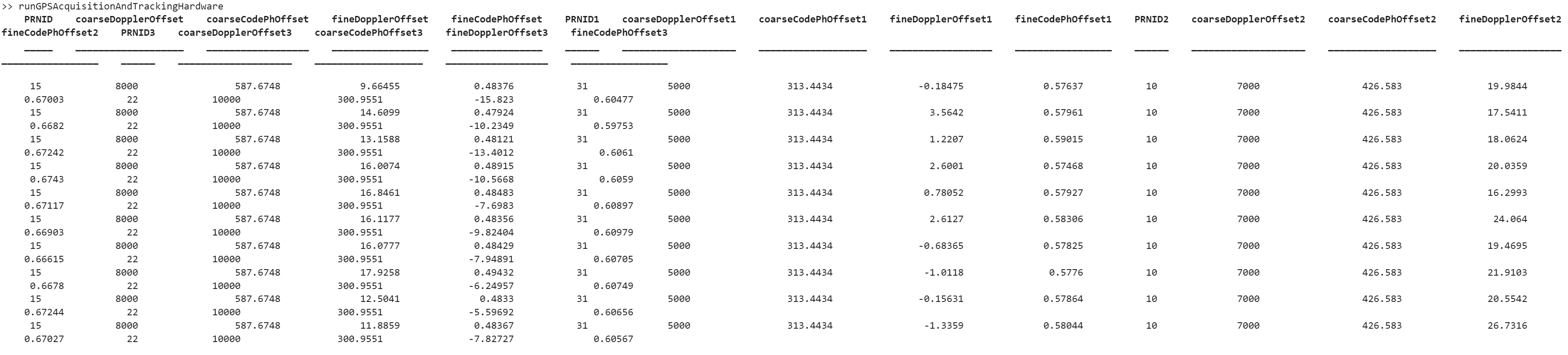
The processor logic contains a read task and a periodic task. The periodic task is a timer-driven task with a periodic time of 1e-2, which is defined in the task manager. The periodic task drives the control and status signals of the hardware algorithm through the AXI4-Lite registers. The model displays status information such as PRNID, coarse code phase offset coarse Doppler offset, fine code phase offset, and fine Doppler offset for 4 satellites from the GPS acquisition and tracking algorithm. The controller provides status information to the MATLAB host by using UDP blocks.
The two tasks are modeled under the Processor Algorithm Periodic subsystem in the processor model soc_GPS_proc and are connected to the Task Manager block at the top level.
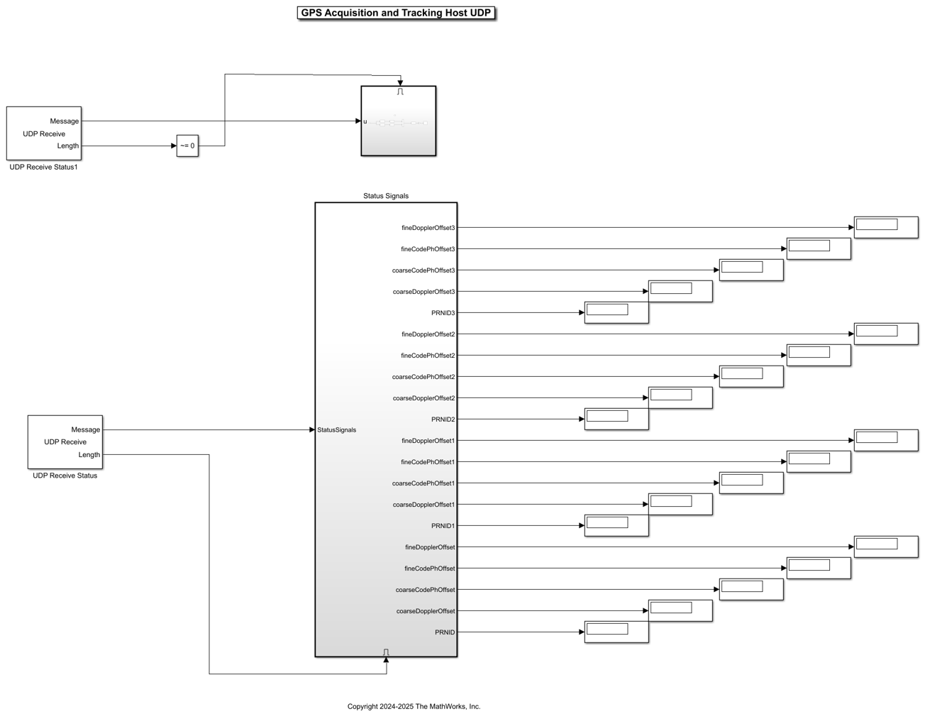
Host Model
The processor sends the GPS Acquisition Tracking subsystem status signals directly back to the host over the Ethernet link by using UDP Write blocks. The IP address of the UDP Write block in the processor model must be configured to the IP address of the host. This interface model, which runs on the host, shows how to receive data from the hardware platform and how to postprocess it.

Simulate
To confirm its basic operation, run the hardware generation model. The model callback runs the soc_GPS_init script to initialize variables required for simulation to the workspace. To access the callback initialization, select MODELING > Model Settings > Model Properties > Callbacks > InitFcn. The simulation result was captured because the soc_GPS_hwtop model contains a large number of HDL-optimized blocks that simulate using sample-based signals, which makes the simulation take a considerable amount of time.
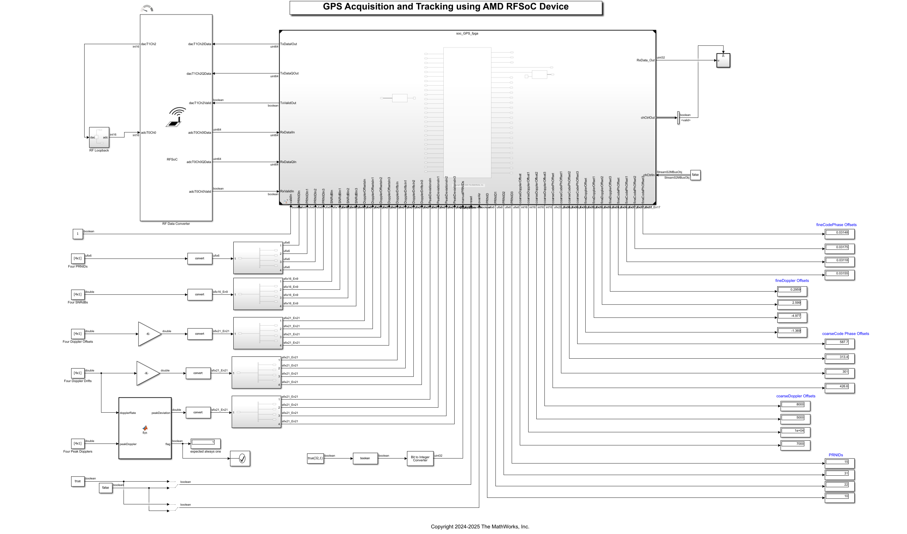
To enable the channel in the GPS waveform 4 satellites subsystem, set OverAir to false. You can control the channel by using channel impairments parameters on the constant blocks Four SNRdBs, Four Doppler Drifts, and Four Doppler Offsets. When you set Over_Air to true, the GPS signals are transmitted and received externally through the ADC, DAC, and RF Data converter. The channel impairments get added externally in real time.
If you want to see the complete hardware and software simulation of the GPS acquisition and tracking algorithm and the controller dynamic configuration, run the soc_GPS_top model. Run the host model to see the status signals.
Implement and Run on Hardware
Hardware Setup
Connect the SMA connector on the XM500 Balun card to complete the loopback between the DAC and ADC, according to these connections: DAC229_T1_CH2 (J5) to ADC224_T0_CH0 (J4).
To implement the model on a supported SoC board, use the SoC Builder tool. Ensure that the Hardware Board option is set to Xilinx Zynq UltraScale+ RFSoC ZCU111 Evaluation Kit on the System on Chip tab of the Simulink toolstrip.
To open SoC Builder, click Configure, Build, & Deploy. After the SoC Builder tool opens, follow these steps.
On the Setup screen, select Build Model and click Next.
On the Select Build Action screen, select Build and load for external mode and then click Next.
On the Select Project Folder screen, specify the project folder and then click Next.
On the Review Memory Map screen, click View/Edit Memory Map to view the memory map and then click Next.
On the Validate Model screen, click Validate to check the compatibility of the model for implementation and then click Next.
On the Build Model screen, click Build to begin building the model. An external shell opens when FPGA synthesis begins. Click Next.
On the Connect Hardware screen, click Test Connection to test the connectivity of the host computer with the SoC board. Click Next to go to the Run Application screen.
FPGA synthesis often takes more than 30 minutes to complete. To save time, you can use the provided pre-generated bitstream by following these steps.
Close the external shell to terminate FPGA synthesis.
Copy the pre-generated bitstream to your project folder by entering this command at the MATLAB command prompt.
copyfile(fullfile(matlabroot, ...
 'toolbox','soc','supportpackages','whdlsocexamples', ...
 'bitstreams','soc_GPS_top-XilinxZynqUltraScale_RFSoCZCU111EvaluationKit.bit'),'./soc_prj');
Click Load and Run to load the pre-generated bitstream and run the model on the SoC board. After the bit file is loaded, open the generated software model.
Run the model in external mode by clicking Monitor & Tune. You can control the configuration from the Simulink model.
Status Signals from Hardware
Run the host model to see the received status signals. When the host interface model runs successfully, the model displays the status signals and LNAV symbol constellation.


Run MATLAB Interface Script
You can control the deployed design using a MATLAB script running on the host. The Prototype Generated IP Core on Hardware using FPGA I/O (HDL Coder) example shows how the HDL Coder™ software generates the interface definition function and the connection between MATLAB and the FPGA. SoC Builder generates the gs_soc_GPS_top_setup function inside the project folder. This function is copied into the runGPSAcquisitionHardware script.
The runGPSAcquisitionAndTrackingHardware script implements the MATLAB control of the deployed design using the generated interface. The script writes control signals to the FPGA, reads results from the FPGA, and displays results in a table.
File Structure
This example uses these files.
Simulink models
soc_GPS_top.slx: Represents the top level SoC implementation of the GPS receiver, connecting the FPGA model,soc_GPS_fpga, to the RF Data Converter and processor model,soc_GPS_proc.soc_GPS_fpga.slx: Represents the algorithm deployed to the FPGA. Implements the GPS acquisition and tracking algorithm and interface logic.soc_GPS_hwtop.slx: Represents the simulation model to verify and validate the algorithm
MATLAB code
runGPSAcquisitionAndTrackingHardware: Implements the FPGA I/O control and runs the GPS algorithm on the hardware.soc_GPS_init,soc_gpshdlAcquisitionAndTrackingUsingCACodeParameters: This MATLAB scripts initialize and generates the parameters required to run the GPS algorithmsoc_HelperGPSNavigationConfig,soc_HelperGPSNAVDataEncode: This MATLAB helpers required to generate the GPS waveform to test the receiver
Further Exploration
This example demonstrated how to integrate the GPS acquisition and tracking algorithm on an AMD ZCU111 evaluation board using an SoC Blockset implementation and how to verify the design in simulation and on hardware. This example is not returning any data decode and position estimation parameters.
To explore further using the GPS HDL Reference Applications Overview (Wireless HDL Toolbox) page, integrate the GPS HDL Acquisition and Tracking Using C/A Code (Wireless HDL Toolbox) example, with the GPS HDL Data Decode and Position Estimation (Wireless HDL Toolbox) example, to run simulations up to position estimation.
This example does not use the embedded processor on the SoC to implement the GPS HDL Data Decode and Position Estimation (Wireless HDL Toolbox) algorithm. It can be further extended to run the position estimation on the processor, thereby realizing a complete GPS receiver SoC implementation on hardware.
See Also
Topics
- GPS HDL Acquisition and Tracking Using C/A Code (Wireless HDL Toolbox)