Read Position of BiSS-C Absolute Encoder
R2026bThis example shows how to read a position of an absolute encoder using the bidirectional serial/synchronous-continuous (BiSS-C) open protocol in the unidirectional mode. This example implements the BiSS-C protocol using TI C2000 peripherals such as CLB, SPI, ePWM, X-BAR, and GPIO using the C2000™ Microcontroller Blockset.
Using this example, you can:
Configure peripheral modules such as CLB, SPI, ePWM, X-BAR, and GPIO to design and implement a BiSS-C protocol.
Generate code for the controller and load it on the hardware board.
Perform Monitor & Tune to monitor the position signals on the host computer.
Run the protocol on F280049C, F28P65x, or F29H85x LaunchPad hardware.
BiSS-C Interface
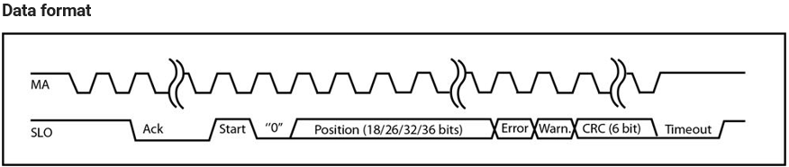
BiSS-C mode (unidirectional) is a fast synchronous serial interface for acquiring position data from an encoder. The controller controls the time of position acquisition and the data transmission speed, and the encoder transfers the position data to the controller.
The interface consists of two unidirectional differential pairs of lines:
Controller clock signals (represented as MA in the diagram) transmits position acquisition requests and timing information (clock) from controller to encoder.
Encoder data out (represented as SLO in the diagram) transfers position data from encoder to controller, synchronized to MA.
This diagram shows the data format for BiSS-C protocol.
Introduction
This example implements the BiSS-C protocol on TI C2000 MCUs (F280049C, F28P65x, F29H85x) using the TI BOOSTXL-POSMGR Position Manager Booster Pack to interface the linear shaft absolute encoder from LinAce. The walkthrough below uses F280049C as the reference; board-specific differences are noted where applicable.
Communication over BiSS-C interface is achieved primarily by CPU (C28x), configurable logic block (CLB), serial peripheral interface (SPI), and device interconnects (X-BARs).
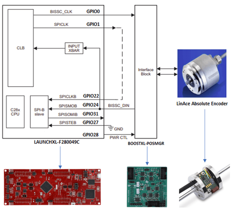
CLB is configured to generate the BiSS-C protocol clock signals (BiSSC_CLK and SPICLK).
BiSS-C protocol clock signals are sent through ePWM channels (GPIO0 &1).
SPI performs the encoder data receive functions.
Input X-BAR is configured to enable the CLB to monitor the SPISIMO signal for detecting the start pulse and accordingly adjusts the phase of the receive clock (SPICLK).
Implementation
The following walkthrough uses the F280049C LaunchPad as reference. For differences in GPIO pins, CLB tile assignments, and configuration files across F28P65x and F29H85x, refer to Connect F280049C LaunchPad to BOOSTXL-POSMGR.
This workflow describes the BiSS-C implementation with respect to the TI F280049C Launchpad.
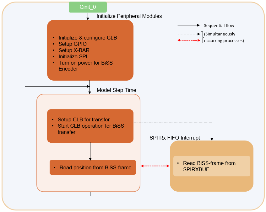
The CPU sets up a CLB for current BiSS-C command depending on the data packet format of the LinAce encoder as shown here:

At each step time in the model, CPU sets up the CLB operation to generate BiSS-C command to read the encoder position.
CLB TILE3 generates a 2MHz reference clock within the CLB module and number of clock pulses (BiSS_CLK-49 pulses and SPICLK-36 pulses), including the edge placement for these two clocks which is precisely controlled by the protocol sequencer tile at this rate.
A SPI interrupt is generated after receiving the data packet from the encoder. CPU then reads and decodes the encoder position from the SPI Receive FIFO.
Note: The protocol sequencer tile varies by device: TILE1 on F280049C, TILE2 on F28P65x, and TILE4 on F29H85x. Clock generation (TILE3) is the same across all platforms.
Required Hardware
This example supports the following hardware boards:
Supported LaunchPads:
Common Accessories:
5V external power supply
Micro-USB cable
Available Models
The following Simulink models are provided:
f280049C_BiSSC_Protocol.slx- F280049C LaunchPadf28p65x_BiSSC_Protocol.slx- F28P65x LaunchPadf29h85x_BiSSC_Protocol.slx- F29H85x LaunchPad
Each model is pre-configured for its target hardware board. Open the model corresponding to your hardware.
Hardware Connections
Connect your target LaunchPad to Texas Instruments BOOSTXL-POSMGR. For more information, refer to Connect F280049C LaunchPad to BOOSTXL-POSMGR.
Connect the Texas Instruments BOOSTXL-POSMGR to BiSS-C Absolute Encoder. For more information, refer to Connect BOOSTXL-POSMGR to Absolute Encoder.
Encoder Connections. For more information, refer to Encoder Connections.
Caution: Double-check 5V and GND connections before powering on to protect the encoder. After power-on, verify three LEDs: D18 (5V supply OK), D16 (PWREN active), and the LinAce green LED (valid data ready).
Model
Open the f280049C_BiSSC_Protocol.slx model. For F28P65x or F29H85x targets, open f28p65x_BiSSC_Protocol.slx or f29h85x_BiSSC_Protocol.slx respectively.
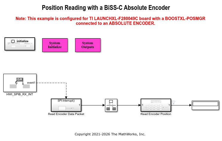
This example demonstrates how to generate the BiSS-C command from the MCU (Controller) to read the position values from the encoder.
Task 1 - Configure and Run Position Reading with a BiSS-C Absolute Encoder Model
1. Open the Simulink model corresponding to your target hardware:
F280049C:
f280049C_BiSSC_Protocol.slxF28P65x:
f28p65x_BiSSC_Protocol.slxF29H85x:
f29h85x_BiSSC_Protocol.slx
2. Each model is pre-configured for its target hardware board. Verify the hardware board setting by pressing Ctrl+E to open Configuration Parameters, then navigate to Hardware Implementation > Hardware board.
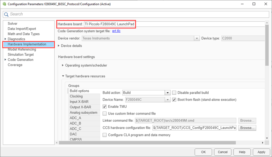
Note: Ensure that the BOOSTXL-POSMGR is connected to the selected hardware board with correct pin mappings.
3. Perform the peripheral configurations in the model as shown in Task 2.
Task 2 - Peripheral Configurations
Set the peripheral block configurations for this model. Double-click the blocks to open block parameter configurations.
CLB Tile, CLB X-BAR, Input X-bar, ePWM are configured to generate BiSS Clock and SPI clock.
CLB
For CLB Tile 1 (F280049C) / Tile 2 (F28P65x) / Tile 4 (F29H85x):
Configure GPREG for Tile boundary IN0 to control the clock generation sequence.
The generated BISSC_CLK and SPICLK clock outputs are routed to the ePWM1A and ePWM1B output pins. The remaining tile boundary configurations are explained in the subsequent sections.
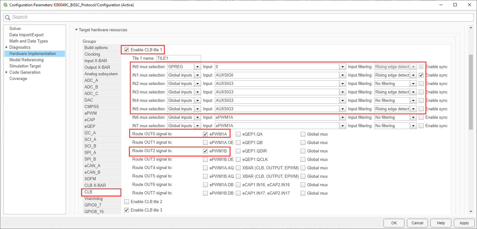
For CLB Tile 3 (all boards):
GPREG settings for TILE3 boundary IN0
TILE3 OUT4 is routed to Global Mux which then is configured in CLB X-BAR to be used by the protocol sequencer tile.
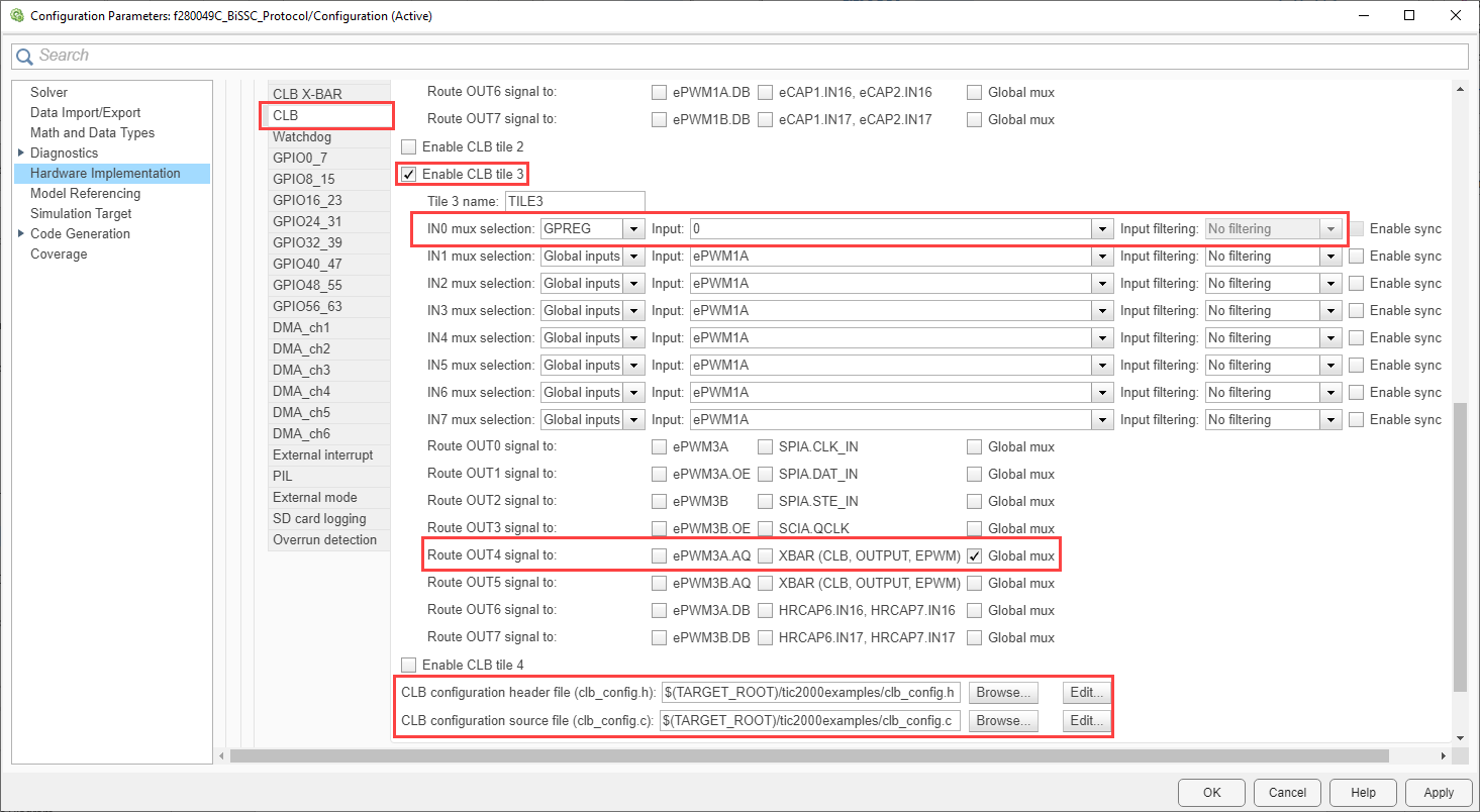
The CLB configuration files, that is the header file and the source file generated from the CCS CLB config tool, are imported into the Simulink model. For more information on how to configure the header file and the source file, see Generate CLB Logic Using SysCfg Tool. For more information on the CLB logic utilized in this example, see CLB Logic for Clock Generation.
Board-Specific CLB Configuration Files:
F280049C:
clb_config.c,clb_config.h(root folder). Protocol sequencer on TILE1.F28P65x:
p65x/clb_config.c,p65x/clb_config.h. Protocol sequencer on TILE2.F29H85x:
f29x/clb_config.c,f29x/clb_config.h. Protocol sequencer on TILE4.
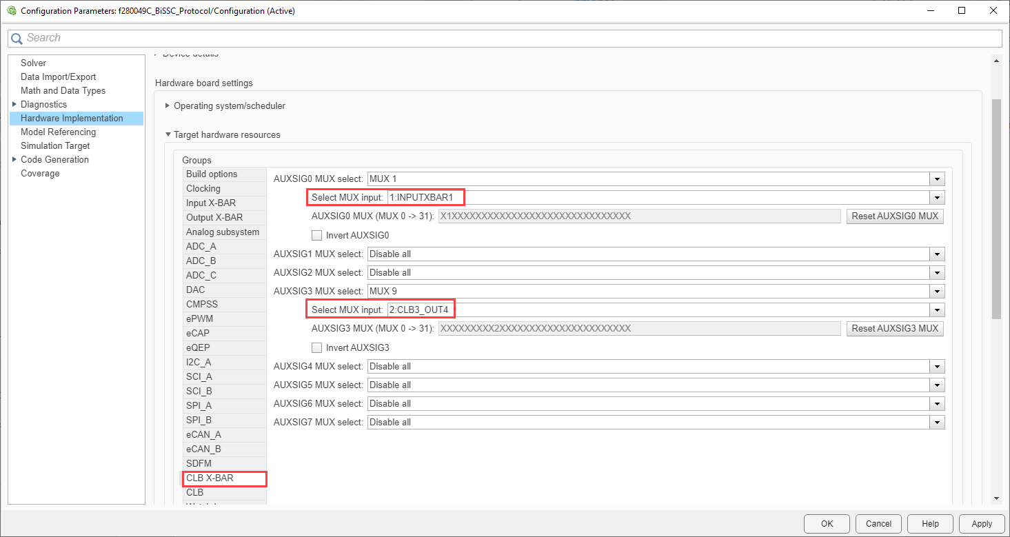
CLB X-BAR
AUXSIG0 Mux select is configured to connect the INPUTXBAR1 i.e BISSC_DIN line to the input of the protocol sequencer tile BOUNDARY IN1.
AUXSIG3 Mux select is configured to connect the CLB3_OUT4 (clock source of 2MHz) to the input of the protocol sequencer tile BOUNDARY in2, in3, in4 and in5.
Input X-BAR
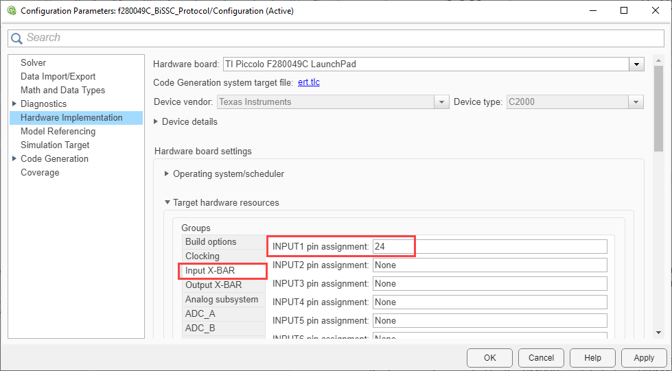
SPIB_SIMO on GPIO24(BISSC_DIN) line over which encoder response is generated is configured in INPUT X-BAR INPUT1.
This setting enables encoder start pulse to be read inside the protocol sequencer tile by FSM_1 followed by FSM_2 to trigger COUNTER_2 to generate the SPICLK clock cycles to read the data packet.
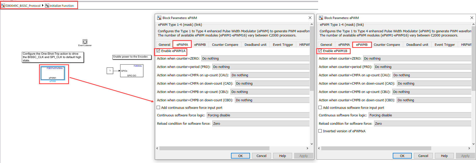
ePWM Block
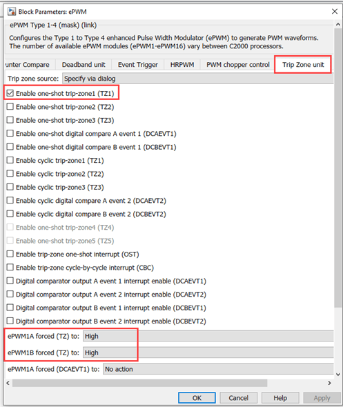
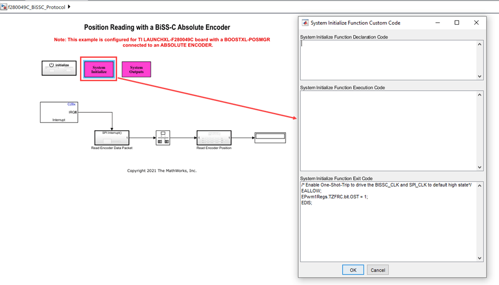
Configure ePWM One Shot Trip option to drive the outputs GPIO0 (ePWM1A) and GPIO1 (ePWM1B) to high state i.e the idle state for output.
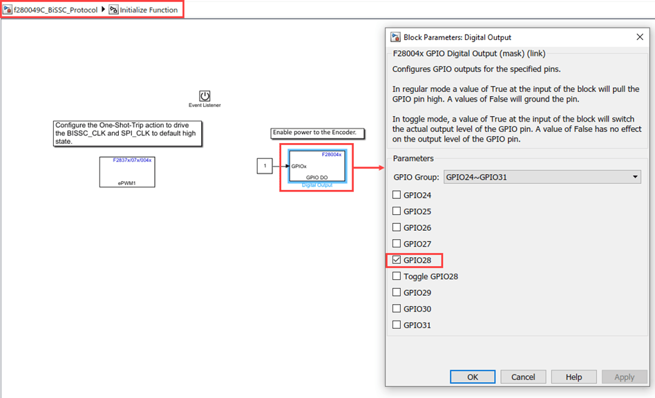
GPIO Block
Enable the power to the encoder. Configure the encoder enable GPIO output pin High to drive the encoder. The pin varies by board: GPIO28 (F280049C), GPIO38 (F28P65x), GPIO70 (F29H85x).
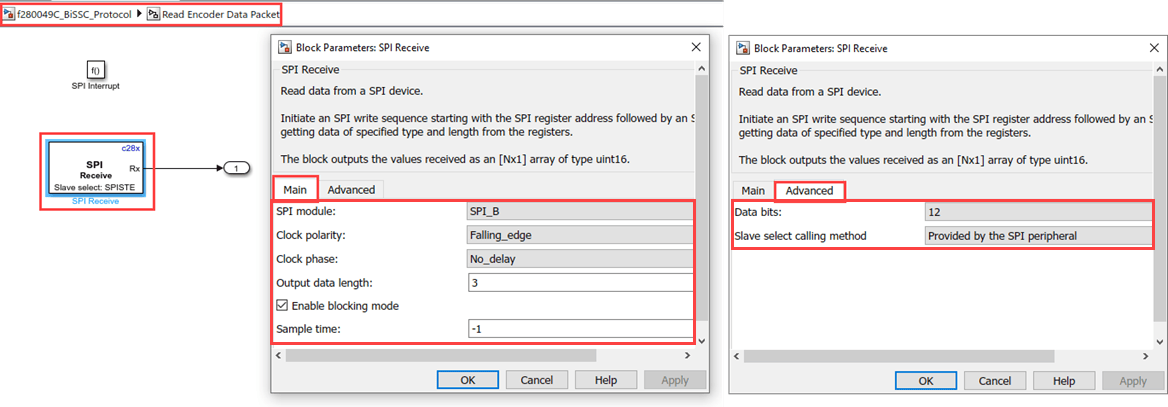
SPI Block
Configure the SPI block to read the encoder position. The SPI is configured to receive 3 words of 12 bits each, totalling 36 bits based on the BiSS-C data packet format shown earlier (Start + CDS + 26-bit Position + Error + Warning + 6-bit CRC).
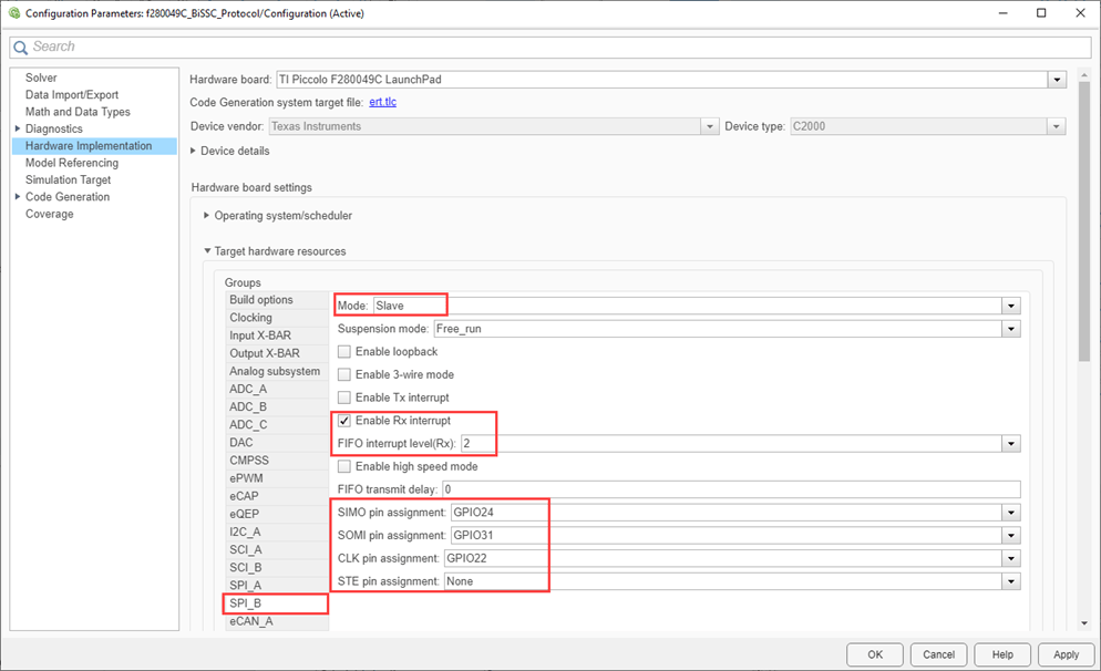
Note: For SPI configuration, the STE pin on the BOOSTXL-POSMGR is connected to ground. Hence the pin is uninitialized from MCU.
Task 3 - CLB Logic for Clock Generation
In this task you will learn how to:
UpdateorModifythe CLB Tile configurations. For more information, see CLB Tile Configuration.Generate CLB configuration file. For more information, see Generate CLB Configuration File.
Generate CLB configuration HTML file. For more information, see Generate CLB Configuration in HTML.
Task 4 - Monitor Signals and Tune the Model
When you perform Monitor & Tune action for the model, the host computer communicates with the target on which the generated executable runs.
Note: The following Monitor & Tune steps are demonstrated using TI F280049C hardware. For F28P65x and F29H85x, refer to the respective LaunchPad user guides for UART pin routing.
Note: Before running Monitor & Tune, verify that the CLB configuration file paths (clb_config.c and clb_config.h) are correctly set in the CLB tab of Configuration Parameters for your target board. Refer to the Board-Specific CLB Configuration Files section in Task 2.
Prerequisites
Before executing Monitor & Tune, perform the following SCI configuration and Dip switch configuration.
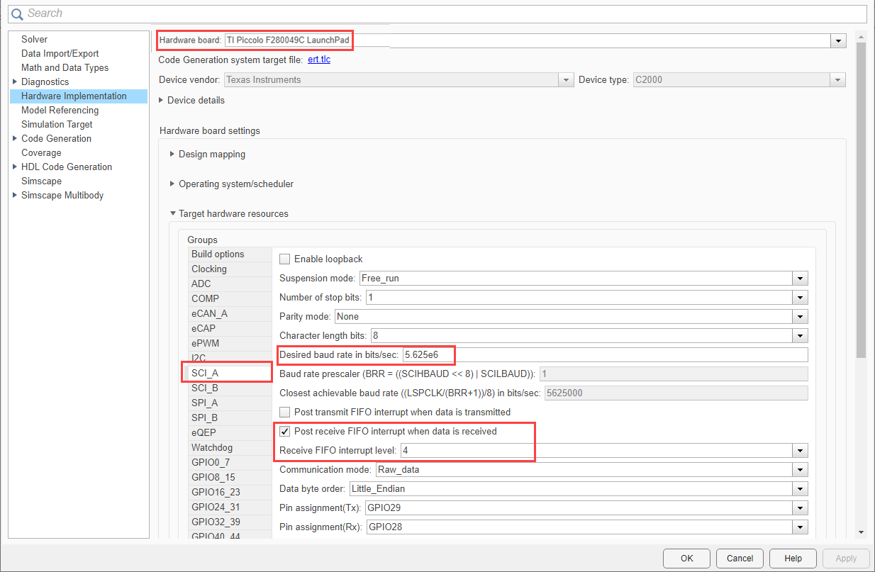
SCI Configuration
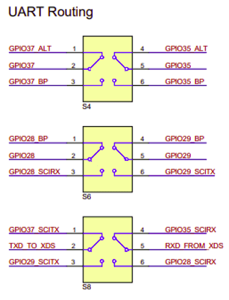
As the encoder enable GPIO (GPIO28 on F280049C) is used to enable the power to the encoder, use GPIO 35 or GPIO37 for UART to run the external mode on F280049C.
Dip Switch Configuration (F280049C Only)
Note: The following dip switch configuration applies only to the F280049C LaunchPad. These settings are not applicable to F28P65x and F29H85x LaunchPads.
Configure the dip switch to the following:
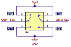
1. Dip switch S3, S4, S8: GPIO35 and GPIO37 routed to the virtual COM port for external mode operation.
2. Dip switch S6: Route the GPIO28-29 to BoosterPack Header. GPIO28 now enables the power to Encoder.
1. Open the Hardware tab and click Monitor & Tune. You can observe from the Diagnostic Viewer that the code is generated for the model and the host connects to the target after loading the generated executable.
Monitor Signals
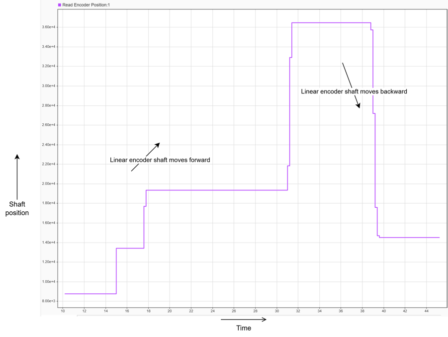
While the model runs, you can monitor the following signals on the Display block. You can monitor the position counts of absolute encoder in the Display block. The following figure shows the encoder position signal logged using the Simulation Data Inspector (SDI). The position remains constant when the encoder shaft is stationary, and changes when the shaft is moved forward or backward.
Troubleshooting
For troubleshooting clock generation, signal routing, pin assignments, and SPI data integrity issues, refer to:
To understand how the CLB and CLB XBAR are configured for debugging, refer to:
Other Things to Try
BOOSTXL-POSMGR supports interfacing up to 2 encoders. A second encoder can be interfaced with a similar approach.
Perform Cyclic Redundancy Check (CRC) on the position data.
Try running the example on F28P65x and F29H85x LaunchPads using the pre-configured models (
f28p65x_BiSSC_Protocol.slxandf29h85x_BiSSC_Protocol.slx) included in this example.

