FPGA-Based Wireless System Design
By Narinder Lall, Xilinx, Inc.
As the market for wireless infrastructure matures equipment vendors are under increasing pressure to deliver low-cost solutions to operators. With today’s complex and rapidly evolving wireless technologies, cost of ownership is typically influenced by both initial capital investment and the ongoing cost of upgrading field installations. Solutions based on digital signal processors (DSPs) and field programmable gate arrays (FPGAs) are attractive because they enable upgrade installation over a network from a central site.
Wireless system designs often feature FPGAs alongside DSPs. FPGAs offer superior speed—even sophisticated algorithms can operate at sample rates of tens or hundreds of MHz. This kind of processing power makes it possible to use FPGAs for implementing not only conventional baseband functionality but also high-speed signal processing that operates close to the antenna. Moreover, FPGAs let engineers optimize fixed-point word lengths and pack multiple channels into a single device, thereby reducing the effective power and cost per channel.
Besides their field programmability, speed, and flexibility, FPGAs also lend themselves to rapid design and verification. In this article, we demonstrate an FPGA design flow that uses a combination of the Simulink family of products, Xilinx System Generator for DSP™, and Xilinx FPGAs. Specifically, we focus on a receiver design for a 16-level quadrature amplitude modulation (16-QAM) telemetry system.
Using Model-Based Design, we can develop a high-level abstraction that can be automatically compiled into an efficient FPGA implementation. Moreover, System Generator’s hardware-in-the-loop (HIL) capability enables the co-simulation of FPGA implementations directly within Simulink. This capability provides a straightforward method to verify hardware implementation and accelerate simulations.
We explore the QAM demodulator design in three phases: system design and modeling, automatic hardware generation, and simulation and hardware verification. (The model is available as a free reference design with System Generator.)
System Design and Modeling
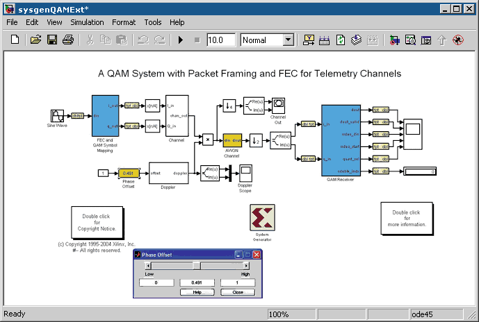
Figure 1 shows a Simulink model of the 16-QAM system design, including transmitter, channel model, and receiver. The transmitter and the receiver sections are modeled in the FEC and QAM Symbol Mapping and QAM Receiver subsystems. This hierarchical approach provides a clean top-level representation, logical grouping of functionality, and a framework for implementation and verification of the design sections.
Transmitter Design
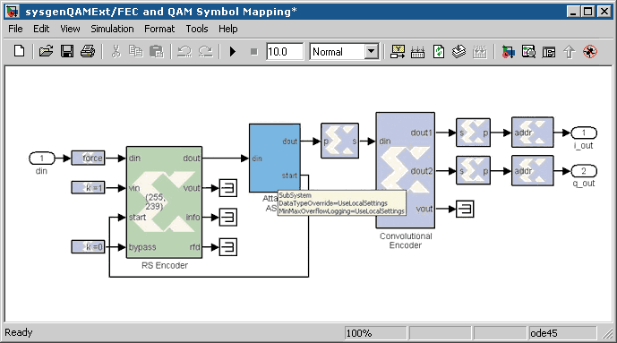
Figure 2 shows the contents of the transmitter subsystem, which processes a stream of 8-bit symbols generated by a sinusoidal test source in the top-level model. The transmitter subsystem performs the following operations:
- Reed-Solomon (RS) encoding—Processes blocks of 239 symbols through an RS encoder, which appends 16 parity symbols to each input block to form 255-symbol code blocks.
- Synchronization marker (ASM)—Prepends a 4-byte ASM to each code block (for non-turbo-coded data, the ASM is 1ACFFC1D in hexadecimal format). The output block size is 259 bytes. The Attach ASM subsystem also generates a start signal for the RS encoder, indicating the beginning of a new code block.
- Convolutional encoding—Converts the symbols into a bit stream and processes it through a convolutional encoder. The Convolutional Encoder block also demultiplexes its encoded bitstream into in-phase and quadrature (I and Q) channels.
- I/Q conversion—Serial to parallel blocks convert the I/Q bitstreams into two 2-bit word streams used to form 16-QAM symbols in the top-level model (one 2-bit word per I/Q rail).
Channel Modeling
The modulated data is passed through a channel model that uses Simulink blocks (Figure 1) to simulate the effects of intersymbol interference, Doppler shifting, and additive white Gaussian noise. The model includes a slider bar that lets you adjust the Doppler shift as the simulation runs to test the receiver’s robustness.
Xilinx gateway input/output blocks representing the pins to the FPGA handle the interface between the transmitter/receiver (fixed point) and the channel model (double precision floating point). Within these blocks, you can specify data type, format, quantization, overflow, and sample period.
Receiver Design
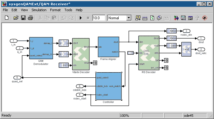
Figure 3 shows the QAM Receiver subsystem. Because our design is destined for an FPGA, it comprises blocks from the System Generator Blockset. The QAM Demodulator subsystem performs QAM demodulation (adaptive equalization, carrier recovery, and slicing), while the rest of the receiver performs Viterbi and RS decoding and frame alignment and includes a controller to resolve QAM phase ambiguity. The Frame Aligner subsystem converts serial data at the Viterbi decoder’s output into bytes that feed the RS decoder. Using pattern-matching circuitry that detects the ASM bit pattern, the Frame Aligner subsystem aligns the serial data so that the first bit of the received ASM becomes the MSB of the corresponding byte output. The match signal is asserted when the last byte of the ASM is presented on the dout port.
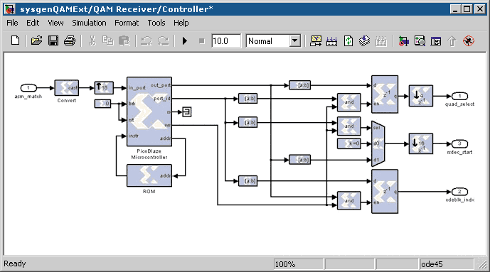
Figure 4 shows the Controller subsystem, which performs periodic 90-degree phase adjustments of the demapped symbols by incrementing the quad_select input of the QAM Demodulator subsystem until the Frame Aligner subsystem detects the ASM pattern. Once synchronization is achieved, the controller asserts the start signal for the RS decoder block. After the entire 255-byte code block is received, the controller ensures that the four ASM bytes are successfully detected in the frame aligner.
Automatic Hardware Generation
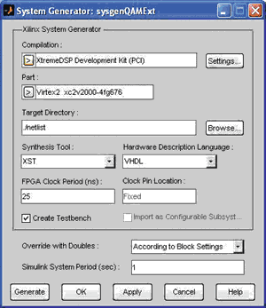
You double-click the System Generator token in the top level of the model to open the hardware generation GUI that lets you specify FPGA family and device, netlist type, Simulink clock rate, and whether a testbench is needed (Figure 5). Clicking Generate produces a cycle- and bit-accurate HDL netlist that can be synthesized and placed-and-routed using Xilinx ISE Foundation FPGA implementation software. System Generator also provides a path to automatically generate an FPGA bit stream (program the FPGA) on the target development board.
Co-Simulation and Hardware Verification
Selecting compilation targets from the Hardware Co-Simulation menu lets you incorporate an implemented design (running on the FPGA) directly within a Simulink simulation. This co-simulation capability automatically creates bit streams to and from the FPGA and associates them with the corresponding System Generator blocks in the Simulink model. Thus, results for the compiled System Generator blocks are computed on the FPGA rather than being emulated in software. Consequently, you can test the design in actual hardware and accelerate the execution of System Generator blocks by a factor of 10–100, typically, saving considerable development and debugging time. Using either the JTAG interface with Parallel Cable IV or specialized interfaces, you can also extend System Generator’s HIL capability to other FPGA platforms.
As an alternative hardware scheme, you can export both the testbench and golden data to hardware description language (HDL) simulation tools that FPGA designers easily understand.
Simulation Acceleration with Simulink
While most of the blocks in this transmitter subsystem come from the System Generator Blockset, you can use similar blocks from the Simulink family of products. For example, the Communications Blockset provides RS encoding and convolutional encoding blocks that could replace the corresponding blocks shown in Figure 2. Each approach has its strengths. In a typical simulation, blocks from the Simulink family of products tend to run faster than their System Generator counterparts, but they generally provide no direct path to an FPGA implementation. System Generator blocks, on the other hand, are designed to provide such an implementation path and also provide a way to accelerate simulations through the HIL capability. Simulink provides a flexible design environment in which you can easily combine blocks depending on where you are in the design process and which design sections are destined for an FPGA.
The Simulink family of products and Xilinx System Generator are widely used together to develop FPGA-based signal processing algorithms for digital communications, video/imaging systems, and aerospace/defense systems. With these tools, system engineers and DSP engineers can rapidly develop algorithms within the Simulink environment and automatically implement their designs on FPGAs. Moreover, System Generator’s HIL capability allows engineers to co-simulate their FPGA implementations directly within Simulink. For the simulation of millions of samples through complex designs, this capability greatly accelerates run speeds and can thus save months of development time.
Consultative Committee for Space Data Systems, “CCSDS 101.0-B-5 Recommendation for Space Data System Standards – Telemetry Channel Coding,” June 2001.
Published 2006
