Hardware Control Signals
Streaming Interface with Valid Signal
DSP System Toolbox™ blocks and functions process matrices of data. In hardware, processing a large matrix of data at one time has a high cost in memory and area. To save resources, serial processing is preferable in HDL designs. DSP HDL Toolbox™ blocks use a streaming sample interface that represents the characteristics of a physical signal. This interface means the blocks operate on one sample at a time, or on a small vector of samples at a time, rather than a large matrix. The blocks accept and return this streaming data accompanied by a control signal that indicates when the data is valid. You can model real-world data patterns such as sample rates or bursty data by using this valid control signal. One valid signal applies to all values in an input or output vector.
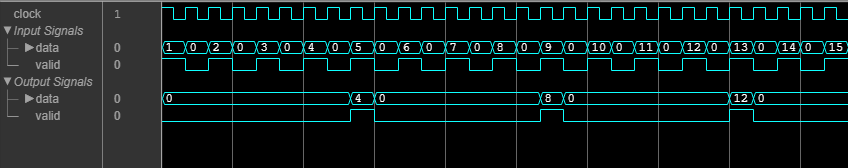
This waveform shows the input and output signals of the Downsampler
block. The block is configured with a downsample rate of 4. The input
data is valid every second cycle. The block downsamples this signal and returns valid
output data every eighth cycle.
You can increase throughput by using frame-based data streams that pass vectors of signals through the blocks and System objects. Frame-based processing increases throughput by implementing the algorithm in parallel on each sample in the input vector. These implementations increase data throughput while using more hardware resources compared to scalar streaming algorithms. Most algorithms in DSP HDL Toolbox support input and output vectors of up to 64 samples, but your vector size might be further limited by the resources available for your design. For details of frame-based support in DSP HDL Toolbox, see High-Throughput HDL Algorithms.
Backpressure Signal
Some DSP HDL Toolbox blocks provide a backpressure output control signal named
ready. The ready signal indicates when the
block has room for a new input sample. This signal is necessary because these blocks
cannot accept new samples when internal storage is full or while performing certain
internal computations, and the latency of those computations can vary with the
configuration of the block.
For example, when you use the burst architecture or the variable-size feature of the
FFT block, you cannot provide the next frame
of input data until memory space is available. For details about the
ready signal for FFT algorithms, see the Control Signals section on the FFT reference
page.
When you use a rate change algorithm or a serial-architecture filter, the blocks use
the ready signal to indicate when they can accept new samples of
input data. When ready is 1
(true), you can apply input data and
valid signals.
Your design can react to the ready signal to decide when to provide
the next input sample, or you can design your system to match the throughput of the
algorithm. To match the throughput, you must leave enough cycles between input samples
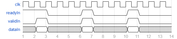
so that the block can process the data. This waveform shows an algorithm that accepts
one sample every four cycles, such as a Discrete FIR Filter configured with a Partly serial
systolic architecture and the Number of cycles
parameter set to 4. The ready signal is high until
a data sample arrives. The ready signal goes low
for three cycles while the block processes the sample, then goes high again. New
data arrives on the fourth cycle, when ready
is high again. The throughput is one sample every four cycles.
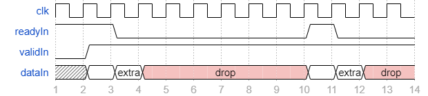
If the upstream part of your design has multiple data samples available and
synchronously reacts to the block setting ready low, then one extra
cycle of input data can arrive at the port. To support synchronous
control logic, such as the HDL FIFO (HDL Coder)
block in Classic mode, the block reserves room to store this
extra data while processing the current data and does not set ready
high until it processes the additional input data. This waveform shows a system that
synchronously releases data in response to ready. The block accepts
one extra cycle of data even though ready is low, and does not set
ready high again until it has processed both inputs. The block
returns the output data in its usual pattern. The throughput is two samples every eight
cycles, the same overall rate as above.

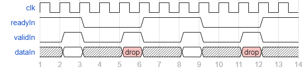
Other than the previous case with the extra cycle, if you send data
while ready is low, the block ignores the data.
This waveform shows a system that sends data every three cycles,
although the block takes four cycles to process one sample. The ready
signal is high and data arrives on cycle 2. The block sets
ready to low on cycle 3. On cycle 5 data
arrives while ready is low and the block ignores it. The block sets
ready to high on cycle 6 when it finishes processing the first
sample. The data sample on cycle 8 arrives while
ready is high, and the block processes it.
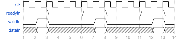
If you wait to detect ready high before releasing the next
data sample, you could lower your throughput. This waveform shows
a system that sends one data sample the cycle after
ready goes high. The throughput is one sample every five cycles,
although the block takes only four cycles to process a sample.
This waveform shows what happens if you hold valid high
regardless of ready. The block accepts two samples and sets
ready low while processing the two samples, then sets
ready high and accepts two more samples. The block ignores any
other samples while ready is low.
The block sets the ready signal high at power-on. When you reset
the design, ready is low for one cycle and then returns to
high.
The Control Data Rate Using Ready Signal example shows how
to use the ready signal with interpolators.
Reset Signal
Most DSP HDL Toolbox blocks provide an optional input reset signal that clears internal states. You can also connect the global reset signal from HDL Coder™ tools to your designs. These are some considerations for using the reset signal options.
By default, the filter blocks connect the generated HDL global reset to only the control path registers. The two reset parameters, Enable reset input port and Use HDL global reset, connect a reset signal to the data path registers. Because of the additional routing and loading on the reset signal, resetting data path registers can reduce synthesis performance.
The Enable reset input port parameter enables the reset port on the block. The reset signal implements a local synchronous reset of the data path registers. For optimal use of FPGA resources, this option does not connect the reset signal to registers targeted to the DSP blocks of the FPGA.
The Use HDL global reset parameter connects the generated HDL global reset signal to the data path registers. This parameter does not change the appearance of the block or modify simulation behavior in Simulink®. The generated HDL global reset can be synchronous or asynchronous depending on the HDL Code Generation > Global Settings > Reset type parameter in the model Configuration Parameters. Depending on your device, using the global reset might move registers out of the DSP blocks and increase resource use.
When you select the Enable reset input port and Use HDL global reset parameters together, the global and local reset signals clear the control and data path registers.
Reset Considerations for Generated Test Benches
FPGA-in-the-loop initialization provides a global reset but does not automatically provide a local reset. With the default reset parameters, the data path registers that are not reset can result in FPGA-in-the-loop (FIL) mismatches if you run the FIL model more than once without resetting the board. Select Use HDL global reset to reset the data path registers automatically, or select Enable reset input port and assert the local reset in your model so the reset signal becomes part of the Simulink FIL test bench.
The generated HDL test bench provides a global reset but does not automatically provide a local reset. With the default reset parameters and the default register reset Configuration Parameters, the generated HDL code includes an initial simulation value for the data path registers. However, if you are concerned about
X-propagation in your design, you can set the HDL Code Generation > Global Settings > Coding style > No-reset registers initialization parameter in Configuration Parameters toDo not initialize. In this case, with the default block reset parameters, the data path registers that are not reset can causeX-propagation on the data path at the start of HDL simulation. Select Use HDL global reset to reset the data path registers automatically, or select Enable reset input port and assert the local reset in your model so the reset signal becomes part of the generated HDL test bench.
Reset Considerations for RAM-Based Partly Serial Architecture
Blocks that implement partly-serial FIR
filters use a RAM-based architecture, which uses fewer resources than a
register-based architecture. Uninitialized RAM locations can result in
X values at the start of your HDL simulation. You can avoid
X values by having your test initialize the RAM or by
enabling the Initialize all RAM blocks option in the model
configuration parameters. This parameter sets the RAM locations to
0 for simulation and is ignored by synthesis tools. Another
option to avoid transient effects from uninitialized RAM locations is to hold reset
for L/M cycles, where L is
the number of coefficients and M is the number of multipliers in
the filter implementation. This operation sets the RAM locations to zeros. (since R2022a)