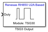
TSG3 Output
generates Pulse Width Modulated (PWM) signals on output pins using the TSG3 peripheral
Since R2026a
Libraries:
Embedded Coder Support Package for Renesas RH850 Microcontrollers /
Renesas RH850 U2A Based
Description
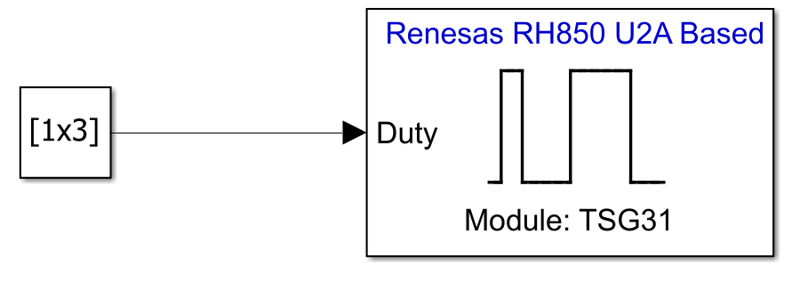
The TSG3 Output block generates Pulse Width Modulated (PWM) signals on output pins using the TSG3 peripheral. You can specify the duty ratios for the three channels (u, v, w) as an array. Each element in the array defines the duty ratio, in percentage, for its corresponding channel.
Note
The TSG3 trigger is currently limited to ADC groups that are mapped to Scan Group 4.
Additionally, trigger routing is fixed per TSG3 instance:
The TSG30 module can trigger only ADCJ0.
The TSG31 module can trigger only ADCJ1.
For information on how to configure the model, AUTOSAR MCAL, and pin mappings to generate PWM signals using TSG3 on the RH850 target, see Getting Started with RH850 TSG3. This tutorial helps with Simulink blocks, model configuration parameters, and MCAL configuration work together to produce hardware PWM output.
The PWM carrier frequency, initial duty-cycle values, duty update timing (peak/valley), dead-time insertion, and ADC trigger events used by this block are configured in the model configuration parameters. For details on these parameters and their impact on PWM generation, see TSG3 in Model Configuration Parameters.
Examples
Control Onboard LED7 Brightness Using TSG3 Blocks on Renesas RH850 Microcontrollers
Control the brightness of an onboard LED7 on the Embedded Coder ® Support Package for Renesas® RH850 Microcontrollers by varying the duty cycle of a TSG3 signal generated using TSG3 blocks. The workflow demonstrates how duty-cycle modulation directly affects LED intensity and how AUTOSAR MCAL configuration integrates with a Simulink model for hardware execution.
Ports
Input
Parameters
Version History
Introduced in R2026a